360 AMD Geode™ SC2200 Processor Data Book
Video Processor Module - Video Processor Registers - Function 4
32580B
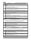
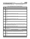
Offset 40h-43h VBI Data Odd Base Register (R/W) Reset Value: 00000000h
This register specifies the base address in graphics memory where VBI data for odd fields are stored. Changes to this register take
effect at the beginning of the next field. The value in this register is 16-byte aligned.
Note: This register is double-buffered. When a new value is written this register, the new value is placed in a special "pending" regis-
ter, and the "Base Register Not Updated" bit (F4BAR2+MemoryOffset 08h[21]) is set to 1. The VBI Data Odd Base Register
(this register) is not updated at this point. When the first data of the next field is stored to memory, the pending values of all
base registers (including this one) are written to the appropriate base registers, and the "Base Register Not Updated" bit is
cleared.
31:0 VBI Odd Base Address. Base address where VBI data for odd fields is stored in graphics memory. Bits [3:0] are always 0
and define the required address space.
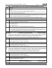
Offset 44h-47h VBI Data Even Base Register (R/W) Reset Value: 00000000h
This register specifies the base address in graphics memory where VBI data for even fields is stored. Changes to this register take effect
at the beginning of the next field. The value in this register is 16-byte aligned.
Note: This register is double-buffered. When a new value is written to this register, the new value is placed in a special "pending" reg-
ister, and the "Base Register Not Updated" bit (F4BAR2+MemoryOffset 08h[21]) is set to 1. The VBI Data Even Base Register
(this register) is not updated at this point. When the first data of the next field is stored to memory, the pending values of all
base registers (including this one) are written to the appropriate base registers, and the "Base Register Not Updated" bit is
cleared.
31:0 VBI Even Base Address. Base address where VBI data for even fields is stored in graphics memory. Bits [3:0] are always
0 and define the required address space.
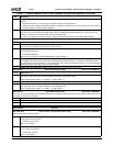
Offset 48h-4Bh VBI Data Pitch Register (R/W) Reset Value: 00000000h
This register specifies the logical width of the VBI data buffer. This value is added to the start of the line address to get the address of the
next line where VBI data are stored to memory. This value must be an integral number of DWORDs.
31:16 Reserved.
15:0 VBI Data Pitch. Specifies the logical width of the video data buffer. Bits [1:0] are always 0.
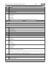
Offset 4Ch-1FFh Reserved Reset Value: 00h
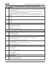
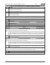
Table 7-8. F4BAR2+Memory Offset: VIP Configuration Registers (Continued)
Bit Description


