


20 AMD Geode™ SC2200 Processor Data Book
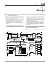
Architecture Overview
32580B
GX_BASE+8408h-840Bh MC_BANK_CFG (R/W) Reset Value: 41104110h
31:16 RSVD (Reserved). Write as 0070h
15 RSVD (Reserved). Write as 0.
14 SODIMM_MOD_BNK (SODIMM Module Banks - Banks 0 and 1). Selects number of module banks installed per SODIMM
for SODIMM:
0: 1 Module bank (Bank 0 only).
1: 2 Module banks (Bank 0 and 1).
13 RSVD (Reserved). Write as 0.
12 SODIMM_COMP_BNK (SODIMM Component Banks - Banks 0 and 1). Selects the number of component banks per
module bank for SODIMM:
0: 2 Component banks.
1: 4 Component banks.
Banks 0 and 1 must have the same number of component banks.
11 RSVD (Reserved). Write as 0.
10:8 SODIMM_SZ (SODIMM Size - Banks 0 and 1). Selects the size of SODIMM:
000: 4 MB 010: 16 MB 100: 64 MB 110: 256 MB
001: 8 MB 011: 32 MB 101: 128 MB 111: 512 MB
This size is the total of both banks 0 and 1. Also, banks 0 and 1 must be the same size.
7 RSVD (Reserved). Write as 0.
6:4 SODIMM_PG_SZ (SODIMM Page Size - Banks 0 and 1). Selects the page size of SODIMM:
000: 1 KB 010: 4 KB 1xx: 16 KB
001: 2 KB 011: 8 KB 111: SODIMM not installed
Both banks 0 and 1 must have the same page size.
3:0 RSVD (Reserved). Write as 0.
GX_BASE+840Ch-840Fh MC_SYNC_TIM1 (R/W) Reset Value: 2A733225h
31 RSVD (Reserved). Write as 0.
30:28 LTMODE (CAS Latency). CAS latency is the delay, in SDRAM clock cycles, between the registration of a read command
and the availability of the first piece of output data. This parameter significantly affects system performance. Optimal setting
should be used. If an SODIMM is used, BIOS can interrogate EEPROM across the ACCESS.bus interface to determine this
value:
000: Reserved 010: 2 CLK 100: 4 CLK 110: 6 CLK
001: Reserved 011: 3 CLK 101: 5 CLK 111: 7 CLK
This field will not take effect until SDRAMPRG (bit 0 of MC_MEM_CNTRL1) transitions from 0 to 1.
27:24 RC (RFSH to RFSH/ACT Command Period, tRC). Minimum number of SDRAM clock between RFSH and RFSH/ACT
commands:
0000: Reserved 0100: 5 CLK 1000: 9 CLK 1100: 13 CLK
0001: 2 CLK 0101: 6 CLK 1001: 10 CLK 1101: 14 CLK
0010: 3 CLK 0110: 7 CLK 1010: 11 CLK 1110: 15 CLK
0011: 4 CLK 0111: 8 CLK 1011: 12 CLK 1111: 16 CLK
23:20 RAS (ACT to PRE Command Period, tRAS). Minimum number of SDRAM clocks between ACT and PRE commands:
0000: Reserved 0100: 5 CLK 1000: 9 CLK 1100: 13 CLK
0001: 2 CLK 0101: 6 CLK 1001: 10 CLK 1101: 14 CLK
0010: 3 CLK 0110: 7 CLK 1010: 11 CLK 1110: 15 CLK
0011: 4 CLK 0111: 8 CLK 1011: 12 CLK 1111: 16 CLK
19 RSVD (Reserved). Write as 0.
18:16 RP (PRE to ACT Command Period, tRP). Minimum number of SDRAM clocks between PRE and ACT commands:
000: Reserved 010: 2 CLK 100: 4 CLK 110: 6 CLK
001: 1 CLK 011: 3 CLK 101: 5 CLK 111: 7 CLK
15 RSVD (Reserved). Write as 0.
14:12 RCD (Delay Time ACT to READ/WRT Command, tRCD). Minimum number of SDRAM clock between ACT and READ/
WRT commands. This parameter significantly affects system performance. Optimal setting should be used:
000: Reserved 010: 2 CLK 100: 4 CLK 110: 6 CLK
001: 1 CLK 011: 3 CLK 101: 5 CLK 111: 7 CLK
Table 2-2. SC2200 Memory Controller Registers (Continued)
Bit Description