AMD Geode™ SC2200 Processor Data Book 63
Signal Definitions
32580B
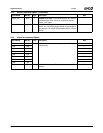
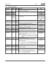
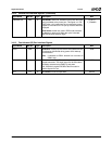
3.4.9 IDE Interface Signals
Signal Name Ball No. Type Description Mux
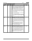
IDE_RST# AA1 O IDE Reset. This signal resets all the devices that are
attached to the IDE interface.
TFTDCK
IDE_ADDR2 U2 O IDE Address Bits. These address bits are used to
access a register or data port in a device on the IDE bus.
TFTD4
IDE_ADDR1 AE1 TFTD2
IDE_ADDR0 AD3 TFTD3
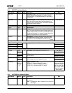
IDE_DATA[15:0] See
Table 3-3
on page
41.
I/O IDE Data Lines. IDE_DATA[15:0] transfers data to/from
the IDE devices.
The IDE interface is
muxed with the TFT
interface. See Table
3-5 on page 46 for
details.
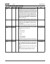
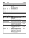
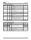
IDE_IOR0# Y4 O IDE I/O Read Channels 0 and 1. IDE_IOR0# is the read
signal for Channel 0 and IDE_IOR1# is the read signal
for Channel 1. Each signal is asserted at read accesses
to the corresponding IDE port addresses.
TFTD10
IDE_IOR1# D28 O GPIO6+DTR2#/
BOUT2+SDTEST5
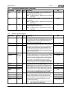
IDE_IOW0# AD2 O IDE I/O Write Channels 0 and 1. IDE_IOW0# is the
write signal for Channel 0. IDE_IOW1# is the write signal
for Channel 1. Each signal is asserted at write accesses
to corresponding IDE port addresses.
TFTD9
IDE_IOW1# C28 O GPIO9+DCD2#+
SDTEST2
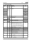
IDE_CS0# AF2 O IDE Chip Selects 0 and 1. These signals are used to
select the command block registers in an IDE device.
TFTD5
IDE_CS1# P2 O TFTDE
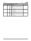
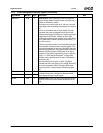
IDE_IORDY0 AD1 I I/O Ready Channels 0 and 1. When de-asserted, these
signals extend the transfer cycle of any host register
access if the required device is not ready to respond to
the data transfer request.
Note: If selected as IDE_IORDY0 or IDE_IORDY1
function(s) but not used, then signal(s) should be
tied high.
TFTD11
IDE_IORDY1 B29 I GPIO10+DSR2#+
SDTEST1
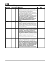
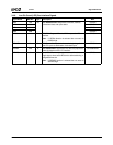
IDE_DREQ0 AC4 I DMA Request Channels 0 and 1. The IDE_DREQ sig-
nals are used to request a DMA transfer from the
SC2200. The direction of transfer is determined by the
IDE_IOR/IOW signals.
Note: If selected as IDE_DREQ0/ IDE_DREQ1 func-
tion but not used, tie IDE_DREQ0/IDE_DREQ1
low.
TFTD8
IDE_DREQ1 C31 I GPIO8+CTS2#
+SDTEST4
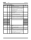
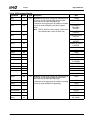
IDE_DACK0# AD4 O DMA Acknowledge Channels 0 and 1. The
IDE_DACK# signals acknowledge the DREQ request to
initiate DMA transfers.
TFTD0
IDE_DACK1# C30 O GPIO7+RTS2#
+SDTEST0
IRQ14 AF1 I Interrupt Request Channels 0 and 1. These input sig-
nals are edge-sensitive interrupts that indicate when the
IDE device is requesting a CPU interrupt service.
Note: If selected as IRQ14/IRQ15 function but not
used, tie IRQ14/IRQ15 low.
TFTD1
IRQ15 AJ8 I GPIO11+RI2#


