248 AMD Geode™ SC2200 Processor Data Book
Core Logic Module - SMI Status and ACPI Registers - Function 1
32580B
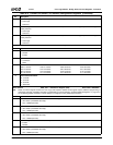
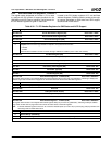
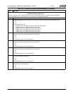
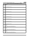
10 SMI Source is EXT_SMI[7:0]. (Read Only. Read Does Not Clear) Indicates whether or not an SMI was caused by a neg-
ative-edge event on EXT_SMI[7:0].
0: No.
1: Yes.
The next level (second level) of SMI status is at F1BAR0+I/O Offset 24h[23:8].
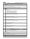
9 SMI Source is General Timers/Traps. (Read Only, Read Does Not Clear) Indicates whether or not an SMI was caused
by the expiration of one of the General Purpose Timers or one of the User Defined Traps.
0: No.
1: Yes.
The next level (second level) of SMI status is at F1BAR0+I/O Offset 04h/06h.
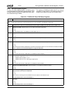
8 SMI Source is Software Generated. (Read to Clear) Indicates whether or not an SMI was caused by software.
0: No.
1: Yes.
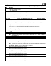
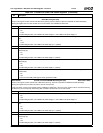
7 SMI on an A20M# Toggle. (Read to Clear) Indicates whether or not an SMI was caused by an access to either Port 92h or
the keyboard command which initiates an A20M# SMI.
0: No.
1: Yes.
This method of controlling the internal A20M# in the GX1 module is used instead of a pin.
To enable SMI generation, set F0 Index 53h[0] to 1.
6 SMI Source is a VGA Timer Event. (Read to Clear) Indicates whether or not an SMI was caused by expiration of the VGA
Timer (F0 Index 8Eh).
0: No.
1: Yes.
To enable SMI generation, set F0 Index 83h[3] to 1.
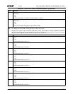
5 SMI Source is Video Retrace. (Read to Clear) Indicates whether or not an SMI was caused by a video retrace event as
decoded from the internal serial connection (PSERIAL register, bit 7) from the GX1 module.
0: No.
1: Yes.
To enable SMI generation, set F0 Index 83h[2] to 1.
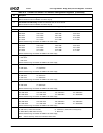
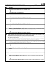
4 Reserved. Reads as 0.
3 SMI Source is LPC. (Read Only, Read Does Not Clear) Indicates whether or not an SMI was caused by the LPC inter-
face.
0: No.
1: Yes.
The next level (second level) of SMI status is at F0BAR1+I/O Offset 1Ch[6:5].
2 SMI Source is ACPI. (Read Only, Read Does Not Clear) Indicates whether or not an SMI was caused by an access (read
or write) to one of the ACPI registers (F1BAR1).
0: No.
1: Yes.
The next level (second level) of SMI status is at F1BAR0+I/O Offset 20h.
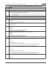
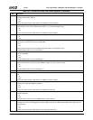
1 SMI Source is Audio Subsystem. (Read Only, Read Does Not Clear) Indicates whether or not an SMI was caused by
the audio subsystem.
0: No.
1: Yes.
The second level of status is found in F3BAR0+Memory Offset 10h/12h.
0 SMI Source is Power Management Event. (Read Only, Read Does Not Clear) Indicates whether or not an SMI was
caused by one of the power management resources (except for GP timers, UDEFx and PCI/ISA function traps which are
reported in bit 9).
0: No.
1: Yes.
The next level (second level) of SMI status is at F0 Index 84h/F4h-87h/F7h.
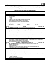
Table 6-33. F1BAR0+I/O Offset: SMI Status Registers (Continued)
Bit Description


