


AMD Geode™ SC2200 Processor Data Book 233
Core Logic Module - Bridge, GPIO, and LPC Registers - Function 0
32580B
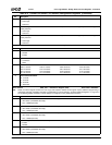
5:0 Signal Select. Selects the GPIO signal to be configured in the Bank selected via bit 5 setting (i.e., Bank 0 or Bank 1). See
Table 4-2 on page 76 for GPIO ball muxing options. GPIOs without an associated ball number are not available externally.
Bank 0
000000 = GPIO0 (ball D11) 010000 = GPIO16 (ball V31)
000001 = GPIO1 (balls D10, N30) 010001 = GPIO17 (ball A10)
000010 = GPIO2 010010 = GPIO18 (ball AG1)
000011 = GPIO3 010011 = GPIO19 (ball C9)
000100 = GPIO4 010100 = GPIO20 (balls A9, N31)
000101 = GPIO5 010101 = GPIO21
000110 = GPIO6 (ball D28) 010110 = GPIO22
000111 = GPIO7 (ball C30) 010111 = GPIO23
001000 = GPIO8 (ball C31) 011000 = GPIO24
001001 = GPIO9 (ball C28) 011001 = GPIO25
001010 = GPIO10 (ball B29) 011010 = GPIO26
001011 = GPIO11 (ball AJ8) 011011 = GPIO27
001100 = GPIO12 (ball N29) 011100 = GPIO28
001101 = GPIO13 (ball M29) 011101 = GPIO29
001110 = GPIO14 (ball D9) 011110 = GPIO30
001111 = GPIO15 (ball A8) 011111 = GPIO31
Bank 1
100000 = GPIO32 (ball M28) 110000 = GPIO48
100001 = GPIO33 (ball L31) 110001 = GPIO49
100010 = GPIO34 (ball L30) 110010 = GPIO50
100011 = GPIO35 (ball L29) 110011 = GPIO51
100100 = GPIO36 (ball L28) 110100 = GPIO52
100101 = GPIO37 (ball K31) 110101 = GPIO53
100110 = GPIO38 (ball K28) 110110 = GPIO54
100111 = GPIO39 (ball J31) 110111 = GPIO55
101000 = GPIO40 (ball Y3) 111000 = GPIO56
101001 = GPIO41 (ball W4) 111001 = GPIO57
101010 = GPIO42 111010 = GPIO58
101011 = GPIO43 111011 = GPIO59
101100 = GPIO44 111100 = GPIO60
101101 = GPIO45 111101 = GPIO61
101110 = GPIO46 111110 = GPIO62
101111 = GPIO47 111111 = GPIO63 (Note)
Note: GPIO63 can be used to generate the PWRBTN# input signal. See PWRBTN# signal description in Section 3.4.15
"Power Management Interface Signals" on page 68.
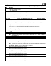
Offset 24h-27h GPIO Signal Configuration Access Register (R/W) Reset Value: 00000044h
This register is used to indicate configuration for the GPIO signal that is selected in the GPIO Signal Configuration Select Register
(above).
Note: PME debouncing, polarity, and edge/level configuration is only applicable on GPIO0-GPIO15 signals (Bank 0 = 00000 to
01111) and on GPIO32-GPIO47 signals (Bank 1 settings of 00000 to 01111). The remaining GPIOs (GPIO16-GPIO31 and
GPIO48-GPIO63) can not generate PMEs, therefore these bits have no function and read 0.
31:7 Reserved. Must be set to 0.
6 PME Debounce Enable. Enables/disables IRQ debounce (debounce period = 16 ms).
0: Disable.
1: Enable. (Default)
See the note in the description of this register for more information about the default value of this bit.
5 PME Polarity. Selects the polarity of the signal that issues a PME from the selected GPIO signal (falling/low or rising/high).
0: Falling edge or low level input. (Default)
1: Rising edge or high level input.
See the note in the description of this register for more information about the default value of this bit.
Table 6-30. F0BAR0+I/O Offset: GPIO Configuration Registers (Continued)
Bit Description