


200 AMD Geode™ SC2200 Processor Data Book
Core Logic Module - Bridge, GPIO, and LPC Registers - Function 0
32580B
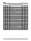
Index 08h Device Revision ID Register (RO) Reset Value: 00h
Index 09h-0Bh PCI Class Code Register (RO) Reset Value: 060100h
Index 0Ch PCI Cache Line Size Register (R/W) Reset Value: 00h
7:0 PCI Cache Line Size Register. This register sets the size of the PCI cache line, in increments of four bytes. For memory
write and invalidate cycles, the PCI cache line size must be set to 32 bytes (08h) and the Memory Write and Invalidate bit
(F0 Index 04h[4]) must be set to 1.
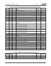
Index 0Dh PCI Latency Timer Register (R/W) Reset Value: 00h
7:4 Reserved. Must be set to 0.
3:0 PCI Latency Timer Value. The PCI Latency Timer register prevents system lockup when a slave does not respond to a
cycle that the Core Logic module masters.
If the value is set to 00h (default), the timer is disabled.
If the timer is written with any other value, bits [3:0] become the four most significant bits in a timer that counts PCI clocks for
slave response.
The timer is reset on each valid data transfer. If the counter expires before the next assertion of TRDY# is received, the
Core Logic module stops the transaction with a master abort and asserts SERR#, if enabled to do so (via F0 Index 04h[8]).
Index 0Eh PCI Header Type (RO) Reset Value: 80h
7:0 PCI Header Type Register. This register defines the format of this header. This header has a format of type 0. (For more
information about this format, see the PCI Local Bus specification, revision 2.2.)
Additionally, bit 7 of this register defines whether this PCI device is a multifunction device (bit 7 = 1) or not (bit 7 = 0).
Index 0Fh PCI BIST Register (RO) Reset Value: 00h
This register indicates various information about the PCI Built-In Self-Test (BIST) mechanism.
Note: This mechanism is not supported in the Core Logic module in the SC2200.
7 BIST Capable. Indicates if the device can run a Built-In Self-Test (BIST).
0: The device has no BIST functionality.
1: The device can run a BIST.
6 Start BIST. Setting this bit to 1 starts up a BIST on the device. The device resets this bit when the BIST is completed. (Not
supported.)
5:4 Reserved.
3:0 BIST Completion Code. Upon completion of the BIST, the completion code is stored in these bits. A completion code of
0000 indicates that the BIST was successfully completed. Any other value indicates a BIST failure.
Index 10h-13h Base Address Register 0 - F0BAR0 (R/W) Reset Value: 00000001h
This register allows access to I/O mapped GPIO runtime and configuration Registers. Bits [5:0] are read only (000001), indicating a 64-
byte aligned I/O address space. Refer to Table 6-30 on page 233 for the GPIO register bit formats and reset values.
31:6 GPIO Base Address.
5:0 Address Range. (Read Only)
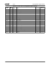
Index 14h-17h Base Address Register 1 - F0BAR1 (R/W) Reset Value: 00000001h
This register allows access to I/O mapped LPC configuration registers. Bits [5:0] are read only (000001), indicating a 64-byte aligned I/O
address space. Refer to Table 6-31 on page 237 for the bit formats and reset values of the LPC registers.
31:6 LPC Base Address.
5:0 Address Range. (Read Only)
Index 18h-2Bh Reserved Reset Value: 00h
Index 2Ch-2Dh Subsystem Vendor ID (RO) Reset Value: 100Bh
Index 2Eh-2Fh Subsystem ID (RO) Reset Value: 0500h
Index 30h-3Fh Reserved Reset Value: 00h
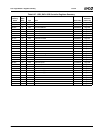
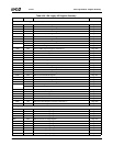
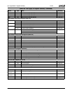
Table 6-29. F0: PCI Header/Bridge Configuration Registers for GPIO and LPC Support (Continued)
Bit Description