224 AMD Geode™ SC2200 Processor Data Book
Core Logic Module - Bridge, GPIO, and LPC Registers - Function 0
32580B
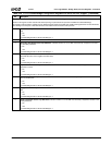
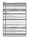
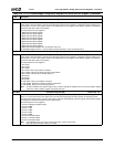
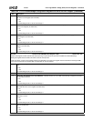
Index B8h DMA Shadow Register (RO) Reset Value: xxh
7:0 DMA Shadow. This 8-bit port sequences through the following list of shadowed DMA Controller registers. At power on, a
pointer starts at the first register in the list and continuing through the other registers in subsequent reads according to the
read sequence. A write to this register resets the read sequence to the first register. Each shadow register in the sequence
contains the last data written to that location.
The read sequence for this register is:
1. DMA Channel 0 Mode Register
2. DMA Channel 1 Mode Register
3. DMA Channel 2 Mode Register
4. DMA Channel 3 Mode Register
5. DMA Channel 4 Mode Register
6. DMA Channel 5 Mode Register
7. DMA Channel 6 Mode Register
8. DMA Channel 7 Mode Register
9. DMA Channel Mask Register (bit 0 is channel 0 mask, etc.)
10. DMA Busy Register (bit 0 or 1 means a DMA occurred within last 1 msec, all other bits are 0)
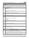
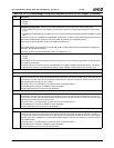
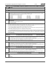
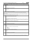
Index B9h PIC Shadow Register (RO) Reset Value: xxh
7:0 PIC Shadow. This 8-bit port sequences through the following list of shadowed Interrupt Controller registers. At power on, a
pointer starts at the first register in the list and continuing through the other registers in subsequent reads according to the
read sequence. A write to this register resets the read sequence to the first register. Each shadow register in the sequence
contains the last data written to that location.
The read sequence for this register is:
1. PIC1 ICW1
2. PIC1 ICW2
3. PIC1 ICW3
4. PIC1 ICW4 - Bits [7:5] of ICW4 are always 0.
5. PIC1 OCW2 - Bits [6:3] of OCW2 are always 0 (See Note).
6. PIC1 OCW3 - Bits [7:4] are 0 and bits [6:3] are 1.
7. PIC2 ICW1
8. PIC2 ICW2
9. PIC2 ICW3
10. PIC2 ICW4 - Bits [7:5] of ICW4 are always 0.
11. PIC2 OCW2 - Bits [6:3] of OCW2 are always 0 (See Note).
12. PIC2 OCW3 - Bits [7:4] are 0 and bits [6:3] are 1.
Note: To restore OCW2 to the shadow register value, write the appropriate address twice. First with the shadow register
value, then with the shadow register value ORed with C0h.
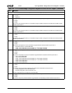
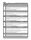
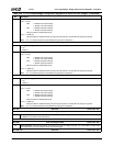
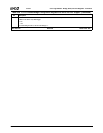
Index BAh PIT Shadow Register (RO) Reset Value: xxh
7:0 PIT Shadow. This 8-bit port sequences through the following list of shadowed Programmable Interval Timer registers. At
power on, a pointer starts at the first register in the list and continuing through the other registers in subsequent reads
according to the read sequence. A write to this register resets the read sequence to the first register. Each shadow register
in the sequence contains the last data written to that location.
The read sequence for this register is:
1. Counter 0 LSB (least significant byte)
2. Counter 0 MSB
3. Counter 1 LSB
4. Counter 1 MSB
5. Counter 2 LSB
6. Counter 2 MSB
7. Counter 0 Command Word
8. Counter 1 Command Word
9. Counter 2 Command Word
Note: The LSB/MSB of the count is the Counter base value, not the current value.
Bits [7:6] of the command words are not used.
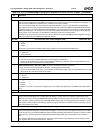
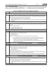
Table 6-29. F0: PCI Header/Bridge Configuration Registers for GPIO and LPC Support (Continued)
Bit Description


