


394 AMD Geode™ SC2200 Processor Data Book
Electrical Specifications
32580B
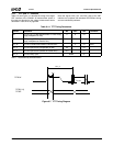
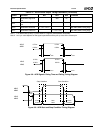
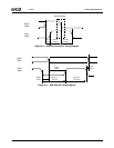
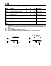
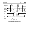
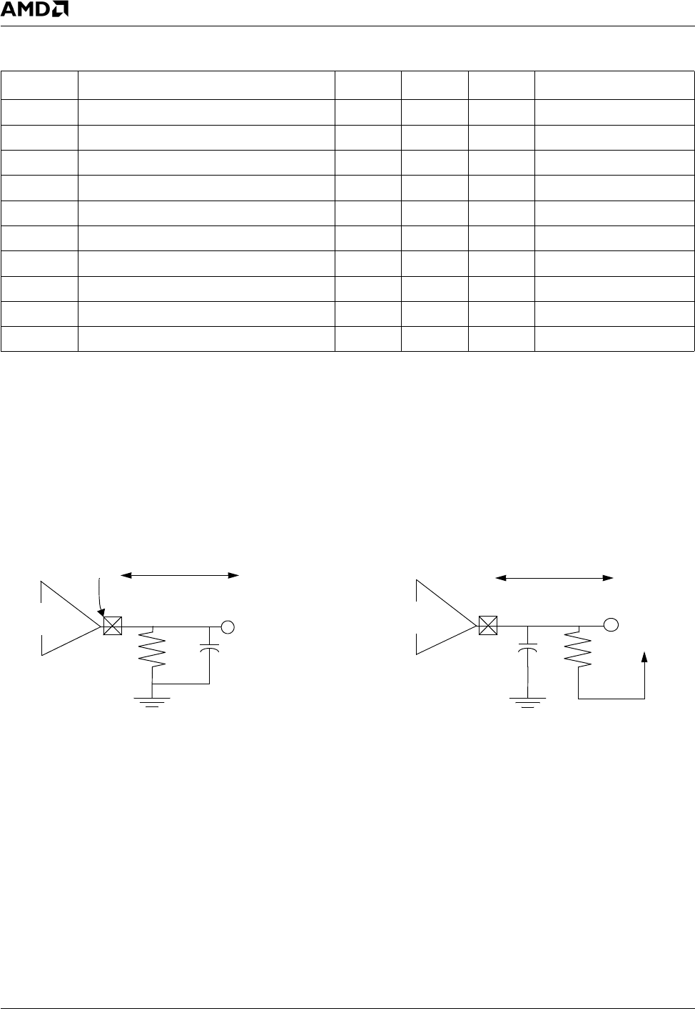
Figure 9-15. Load Circuits for Maximum Time Measurements
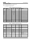
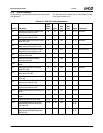
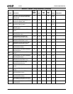
Table 9-20. PCI Timing Parameters
Symbol Parameter Min Max Unit Comments
t
VAL
PCICLK to signal valid delay (on the bus) 2 11 ns Note 1, Note 2
t
VAL
(ptp) PCICLK to signal valid delay (GNT#) 2 9 ns Note 1, Note 2
t
ON
Float to active delay 2 ns Note 1, Note 3,
t
OFF
Active to float delay 28 ns Note 1, Note 3,
t
SU
Input setup time to PCICLK (on the bus) 7 ns Note 4
t
SU
(ptp) Input setup time to PCICLK (REQ#) 6 ns Note 4
t
H
Input hold time from PCICLK 0 ns Note 4
t
RST
PCIRST# active time after power stable 1 ms Note 3, Note 5
t
RST-CLK
PCIRST# active time after PCICLK stable 100 µs Note 3, Note 5
t
RST-OFF
PCIRST# active to output float delay 40 ns Note 3, Note 5, Note 6
Note 1. See the timing measurement conditions in Figure 9-16.
Note 2. Minimum times are evaluated with same load used for slew rate measurement (as shown in note 3 of Table ); max-
imum times are evaluated with the load circuits shown in Figure 9-15, for high-going and low-going edges respec-
tively.
Note 3. Not 100% tested.
Note 4. See the timing measurement conditions in Figure 9-17.
Note 5. PCIRST# is asserted and de-asserted asynchronously with respect to PCICLK (see Figure 9-18).
Note 6. All output drivers are asynchronously floated when PCIRST# is active.
Output
Buffer
Output
Buffer
V
CC
25 Ω
25 Ω
10 pF
10 pF
0.5" max.
0.5" max.
Pin
t
VAL
(Max) Rising Edge
t
VAL
(Max) Falling Edge