


AMD Geode™ SC2200 Processor Data Book 231
Core Logic Module - Bridge, GPIO, and LPC Registers - Function 0
32580B
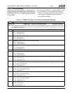
6.4.1.1 GPIO Support Registers
F0 Index 10h, Base Address Register 0 (F0BAR0) points to
the base address of where the GPIO runtime and configu-
ration registers are located. Table 6-29 gives the bit formats
of I/O mapped registers accessed through F0BAR0.
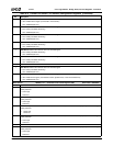
Table 6-30. F0BAR0+I/O Offset: GPIO Configuration Registers
Bit Description
Offset 00h-03h GPDO0 — GPIO Data Out 0 Register (R/W) Reset Value: FFFFFFFFh
31:0 GPIO Data Out. Bits [31:0] of this register correspond to GPIO31-GPIO0 signals, respectively. The value of each bit deter-
mines the value driven on the corresponding GPIO signal when its output buffer is enabled. Writing to the bit latches the
written data unless the bit is locked by the GPIO Configuration register Lock bit (F0BAR0+I/O Offset 24h[3]). Reading the
bit returns the value, regardless of the signal value and configuration.
0: Corresponding GPIO signal is driven to low when output enabled.
1: Corresponding GPIO signal is driven or released to high (according to buffer type and static pull-up selection) when out-
put is enabled.
Offset 04h-07h GPDI0 — GPIO Data In 0 Register (RO) Reset Value: FFFFFFFFh
31:0 GPIO Data In. Bits [31:0] of this register correspond to GPIO31-GPIO0 signals, respectively. Reading each bit returns the
value of the corresponding GPIO signal, regardless of the signal configuration and the GPDO0 register (F0BAR0+I/O Offset
00h) value.
Writes to this register are ignored.
0: Corresponding GPIO signal level is low.
1: Corresponding GPIO signal level is high.
Offset 08h-0Bh GPIEN0 — GPIO Interrupt Enable 0 Register (R/W) Reset Value: 00000000h
31:16 Reserved. Must be set to 0.
15:0 GPIO Power Management Event (PME) Enable. Bits [15:0] correspond to GPIO15-GPIO0 signals, respectively. Each bit
allows PME generation by the corresponding GPIO signal.
0: Disable PME generation.
1: Enable PME generation.
Notes: 1) All of the enabled GPIO PMEs are always reported at F1BAR1+I/O Offset 10h[3].
2) Any enabled GPIO PME can be selected to generate an SCI or SMI at F1BAR1+I/O Offset 0Ch[0].
If SCI is selected, then the individually selected GPIO PMEs are globally enabled for SCI generation at
F1BAR1+I/O Offset 12h[3] and the status is reported at F1BAR1+I/O Offset 10h[3].
If SMI is selected, the individually selected GPIO PMEs generate an SMI and the status is reported at
F1BAR0+I/O Offset 00h/02h[0].
Offset 0Ch-0Fh GPST0 — GPIO Status 0 Register (R/W1C) Reset Value: 00000000h
31:16 Reserved. Must be set to 0.
15:0 GPIO Status. Bits [15:0] correspond to GPIO15-GPIO0 signals, respectively. Each bit reports a 1 when hardware detects
the edge (rising/falling on the GPIO signal) that is programmed in F0BAR0+I/O Offset 24h[5]. If the corresponding bit in
F0BAR0+I/O Offset 08h is set, this edge generates a PME.
0: No active edge detected since the bit was last cleared.
1: Active edge detected.
Writing 1 to the a Status bit clears it to 0.
This is the third level of SMI status reporting to the second level at F0 Index 87h/F7h[7] and the top level at F1BAR0+I/O
Offset 00h/02h[0]. Clearing the third level also clears the second and top levels.
This is the second level of SCI status reporting to the top level at F1BAR1+Offset 10h[3]. The status must be cleared at
both the this level and the top level (i.e., the top level is not automatically cleared when a bit in this register is cleared).
Offset 10h-13h GPDO1 — GPIO Data Out 1 Register (R/W) Reset Value: FFFFFFFFh
31:0 GPIO Data Out. Bits [31:0] of this register correspond to GPIO63-GPIO32 signals, respectively. The value of each bit
determines the value driven on the corresponding GPIO signal when its output buffer is enabled. Writing to the bit latches
the written data unless the bit is locked by the GPIO Configuration register Lock bit (F0BAR0+I/O Offset 24h[3]). Reading
the bit returns the value, regardless of the signal value and configuration.
0: Corresponding GPIO signal driven to low when output enabled.
1: Corresponding GPIO signal driven or released to high (according to buffer type and static pull-up selection) when output
enabled.