


436 AMD Geode™ SC2200 Processor Data Book
Electrical Specifications
32580B
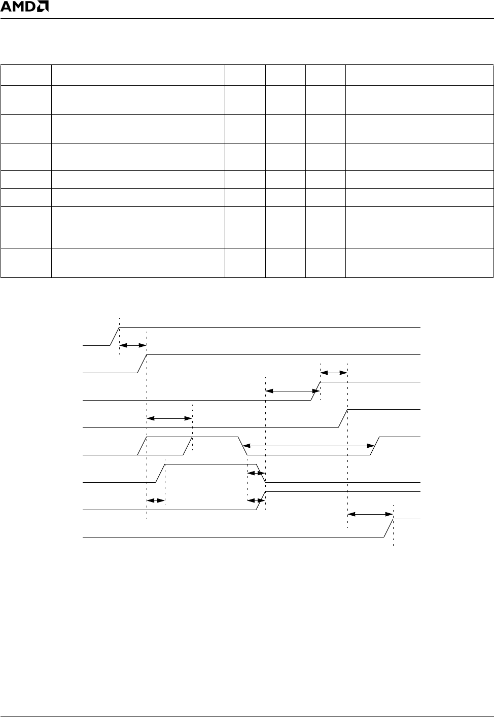
9.3.15 Power-Up Sequencing
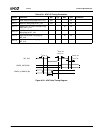
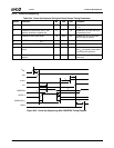
Figure 9-55. Power-Up Sequencing With PWRBTN# Timing Diagram
Table 9-44. Power-Up Sequence Using the Power Button Timing Parameters
Symbol Parameter Min Max Unit Comments
t
1
Voltage sequence -100 100 ms Optimum power-up results with
t
1
= 0.
t
2
PWRBTN# inactive after V
SB
or V
SBL
applied, whichever is applied last
0 1 µs PWRBTN# is an input and must
be powered by V
SB
.
t
3
PWRBTN# active pulse width 16 4000 ms If PWRBTN# max is exceeded,
ONCTL# will go inactive.
t
4
ONCTL# inactive after V
SB
applied 0 1 ms
t
5
Signal active after PWRBTN active 14 16 ms
t
6
V
CORE
and V
IO
applied after ONCTL#
active
0 ms System determines when V
CORE
and V
IO
are applied, hence there
is no maximum constraint.
t
7
POR# inactive after V
CORE
and V
IO
applied
50 ms POR# must not glitch during
active time.
t
1
V
SBL
V
SB
V
CORE
V
IO
PWRBTN#
ONTCL#
PWRCNT[2:1]
POR#
t
4
t
2
t
3
t
1
t
6
t
5
t
7