AMD Geode™ SC2200 Processor Data Book 219
Core Logic Module - Bridge, GPIO, and LPC Registers - Function 0
32580B
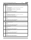
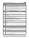
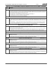
Index 8Ah General Purpose Timer 2 Count Register (R/W) Reset Value: 00h
7:0 GPT2_COUNT. This field represents the load value for General Purpose Timer 2. This value can represent either an 8-bit or
16-bit counter (configured in F0 Index 8Bh[5]). It is loaded into the counter when the timer is enabled (F0 Index 83h[1] = 1).
Once the timer is enabled and a transition occurs on GPIO7, the timer is re-loaded.
The counter is decremented with each clock of the configured timebase (1 msec or 1 sec selected at F0 Index 8Bh[3]).
Upon expiration of the counter, an SMI is generated and the top level of status is F1BAR0+I/O Offset 00h/02h[9]. The sec-
ond level of status is reported at F1BAR0+I/O Offset 04h/06h[1]). Once expired, this counter must be re-initialized by either
disabling and enabling it, or by writing a new count value in this register. See Section 6.2.10.3 "Peripheral Power Manage-
ment" on page 172 for a discussion on the limitations of producing count error with small values.”
For GPIO7 to act as the reload for this counter, it must be enabled as such (F0 Index 8Bh[2]) and be configured as an input.
(GPIO pin programming is at F0BAR0+I/O Offset 20h and 24h.)
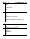
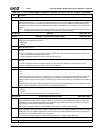
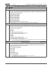
Index 8Bh General Purpose Timer 2 Control Register (R/W) Reset Value: 00h
7 Re-trigger General Purpose Timer 1 (GP Timer 1) on Secondary Hard Disk Activity.
0: Disable.
1: Enable.
Any access to the secondary hard disk address range selected in F0 Index 93h[4] reloads GP Timer 1.
6 VGA Timer Base. Selects timebase for VGA Timer Register (F0 Index 8Eh).
0: 1 millisecond.
1: 32 microseconds.
5 General Purpose Timer 2 (GP Timer 2) Shift. GP Timer 2 is treated as an 8-bit or 16-bit timer.
0: 8-bit. The count value is loaded into GP Timer 2 Count Register (F0 Index 8Ah).
1: 16-bit. The value loaded into GP Timer 2 Count Register is shifted left by eight bits, the lower eight bits become zero,
and this 16-bit value is used as the count for GP Timer 2.
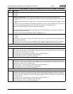
4 General Purpose Timer 1 (GP Timer 1) Shift. GP Timer 1 is treated as an 8-bit or 16-bit timer.
0: 8-bit. The count value is that loaded into GP Timer 1 Count Register (F0 Index 88h).
1: 16-bit. The value loaded into GP Timer 1 Count Register is shifted left by eight bit, the lower eight bits become zero, and
this 16-bit value is used as the count for GP Timer 1.
3 General Purpose Timer 2 (GP Timer 2) Timebase. Selects timebase for GP Timer 2 (F0 Index 8Ah).
0: 1 second.
1: 1 millisecond.
2 Re-trigger Timer on GPIO7 Pin Transition. A rising-edge transition on the GPIO7 pin reloads GP Timer 2 (F0 Index 8Ah).
0: Disable.
1: Enable.
For GPIO7 to work here, it must first be configured as an input. (GPIO pin programming is at F0BAR0+I/O Offset 20h and
24h.)
1:0 Reserved. Set to 0.
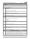
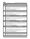
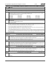
Index 8Ch IRQ Speedup Timer Count Register (R/W) Reset Value: 00h
7:0 IRQ Speedup Timer Load Value. This field represents the load value for the IRQ speedup timer. It is loaded into the
counter when Suspend Modulation is enabled (F0 Index 96h[0] = 1) and an INTR or an access to I/O Port 061h occurs.
When the event occurs, the Suspend Modulation logic is inhibited, permitting full performance operation of the GX1 module.
Upon expiration, no SMI is generated; the Suspend Modulation begins again. The IRQ speedup timer’s timebase is 1 msec.
This speedup mechanism allows instantaneous response to system interrupts for full-speed interrupt processing. A typical
value here would be 2 to 4 msec.
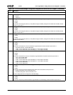
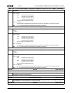
Index 8Dh Video Speedup Timer Count Register (R/W) Reset Value: 00h
7:0 Video Speedup Timer Load Value. This field represents the load value for the Video speedup timer. It is loaded into the
counter when Suspend Modulation is enabled (F0 Index 96[0] = 1) and any access to the graphics controller occurs. When
a video access occurs, the Suspend Modulation logic is inhibited, permitting full-performance operation of the GX1 module.
Upon expiration, no SMI is generated, and Suspend Modulation begins again. The video speedup timer’s timebase is 1
msec.
This speedup mechanism allows instantaneous response to video activity for full speed during video processing calcula-
tions. A typical value here would be 50 msec to 100 msec.
Table 6-29. F0: PCI Header/Bridge Configuration Registers for GPIO and LPC Support (Continued)
Bit Description


