AMD Geode™ SC2200 Processor Data Book 245
Core Logic Module - SMI Status and ACPI Registers - Function 1
32580B
6.4.2 SMI Status and ACPI Registers - Function 1
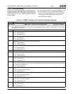
The register space designated as Function 1 (F1) is used
to configure the PCI portion of support hardware for the
SMI Status and ACPI Support registers. The bit formats for
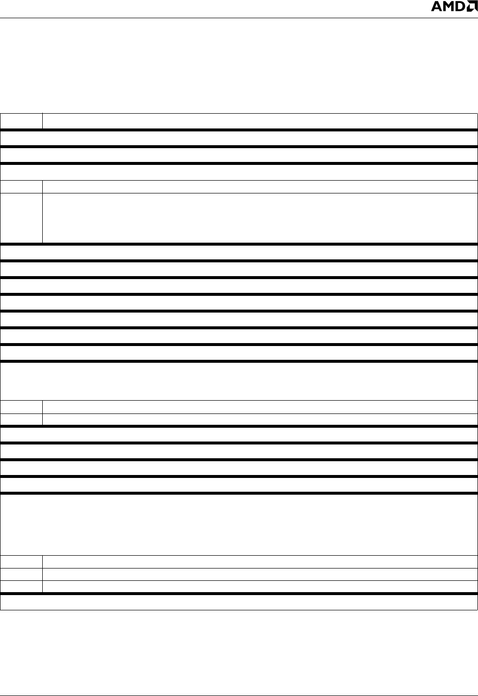
the PCI Header registers are given in Table 6-32.
Located in the PCI Header registers of F1 are two Base
Address Registers (F1BARx) used for pointing to the regis-
ter spaces designated for SMI status and ACPI support,
described later in this section.
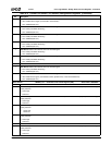
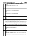
Table 6-32. F1: PCI Header Registers for SMI Status and ACPI Support
Bit Description
Index 00h-01h Vendor Identification Register (RO) Reset Value: 100Bh
Index 02h-03h Device Identification Register (RO) Reset Value: 0501h
Index 04h-05h PCI Command Register (R/W) Reset Value: 0000h
15:1 Reserved. (Read Only)
0 I/O Space. Allow the Core Logic module to respond to I/O cycles from the PCI bus.
0: Disable.
1: Enable.
This bit must be enabled to access I/O offsets through F1BAR0 and F1BAR1 (see F1 Index 10h and 40h).
Index 06h-07h PCI Status Register (RO) Reset Value: 0280h
Index 08h Device Revision ID Register (RO) Reset Value: 00h
Index 09h-0Bh PCI Class Code Register (RO) Reset Value: 068000h
Index 0Ch PCI Cache Line Size Register (RO) Reset Value: 00h
Index 0Dh PCI Latency Timer Register (RO) Reset Value: 00h
Index 0Eh PCI Header Type (RO) Reset Value: 00h
Index 0Fh PCI BIST Register (RO) Reset Value: 00h
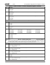
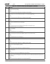
Index 10h-13h Base Address Register 0 - F1BAR0 (R/W) Reset Value: 00000001h
This register allows access to I/O mapped SMI status related registers. Bits [7:0] are read only (0000 0001), indicating a 256-byte I/O
address range. Refer to Table 6-33 on page 246 for bit formats and reset values of the SMI status registers.
31:8 SMI Status Base Address.
7:0 Address Range. (Read Only)
Index 14h-2Bh Reserved Reset Value: 00h
Index 2Ch-2Dh Subsystem Vendor ID (RO) Reset Value: 100Bh
Index 2Eh-2Fh Subsystem ID (RO) Reset Value: 0501h
Index 30h-3Fh Reserved Reset Value: 00h
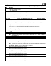
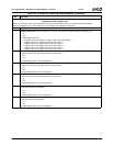
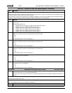
Index 40h-43h Base Address Register 1 - F1BAR1 (R/W) Reset Value: 00000001h
This register allows access to I/O mapped ACPI related registers. Bits [7:0] are read only (0000 0001), indicating a 256 byte address
range. Refer to Table 6-34 on page 255 for bit formats and reset values of the ACPI registers.
Note: This Base Address register moved from its normal PCI Header Space (F1 Index 14h) to prevent plug and play software from
relocating it after an FACP table is built.
31:8 ACPI Base Address.
7:1 Address Range. (Read Only)
0 Enable. (Write Only) This bit must be set to 1 to enable access to ACPI Support Registers.
Index 44h-FFh Reserved Reset Value: 00h


