


18 AMD Geode™ SC2200 Processor Data Book
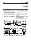
Architecture Overview
32580B
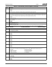
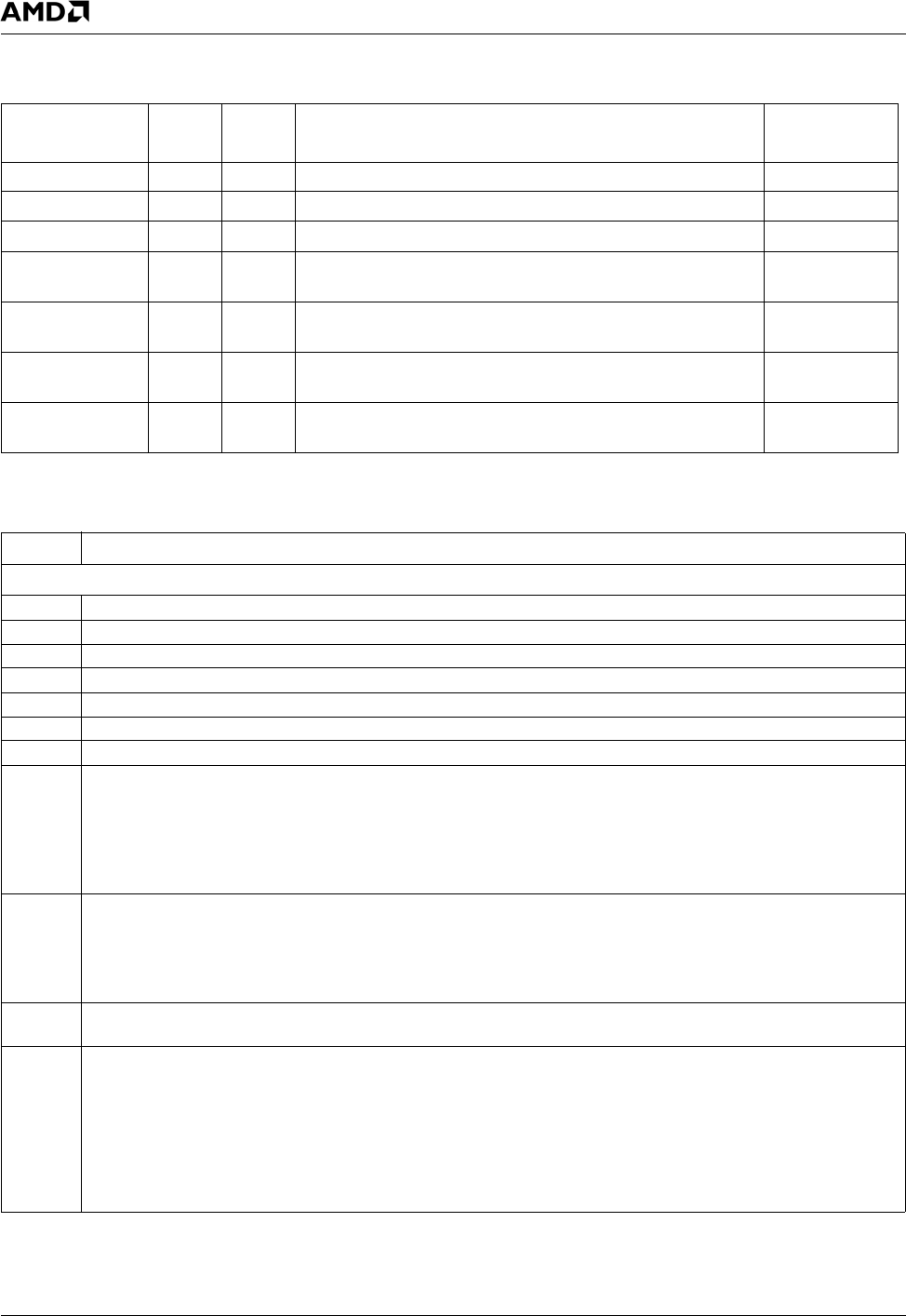
Table 2-1. SC2200 Memory Controller Register Summary
GX_BASE+
Memory Offset
Width
(Bits) Type Name/Function Reset Value
8400h-8403h 32 R/W MC_MEM_CNTRL1. Memory Controller Control Register 1 248C0040h
8404h-8407h 32 R/W MC_MEM_CNTRL2. Memory Controller Control Register 2 00000801h
8408h-840Bh 32 R/W MC_BANK_CFG. Memory Controller Bank Configuration 41104110h
840Ch-840Fh 32 R/W MC_SYNC_TIM1. Memory Controller Synchronous Timing
Register 1
2A733225h
8414h-8417h 32 R/W MC_GBASE_ADD. Memory Controller Graphics Base
Address Register
00000000h
8418h-841Bh 32 R/W MC_DR_ADD. Memory Controller Dirty RAM Address
Register
00000000h
841Ch-841Fh 32 R/W MC_DR_ACC. Memory Controller Dirty RAM Access
Register
0000000xh
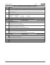
Table 2-2. SC2200 Memory Controller Registers
Bit Description
GX_BASE+ 8400h-8403h MC_MEM_CNTRL1 (R/W) Reset Value: 248C0040h
31:30 MDCTL (MD[63:0] Drive Strength). 11 is strongest, 00 is weakest.
29 RSVD (Reserved) Write as 0.
28:27 MABACTL (MA[12:0] and BA[1:0] Drive Strength). 11 is strongest, 00 is weakest.
26 RSVD (Reserved). Write as 0.
25:24 MEMCTL (RASA#, CASA#, WEA#, CS[1:0]#, CKEA, DQM[7:0] Drive Strength). 11 is strongest, 00 is weakest.
23:22 RSVD (Reserved). Write as 0.
21 RSVD (Reserved). Must be written as 0. Wait state on the X-Bus x_data during read cycles - for debug only.
20:18 SDCLKRATE (SDRAM Clock Ratio). Selects SDRAM clock ratio.
000: Reserved 100: ÷ 3.5
001: ÷ 2 101: ÷ 4
010: ÷ 2.5 110: ÷ 4.5
011: ÷ 3 (Default) 111: ÷ 5
Ratio does not take effect until the SDCLKSTRT bit (bit 17 of this register) transitions from 0 to 1.
17 SDCLKSTRT (Start SDCLK). Start operating SDCLK using the new ratio and shift value (selected in bits [20:18] of this reg-
ister).
0: Clear.
1: Enable.
This bit must transition from zero (written to zero) to one (written to one) in order to start SDCLK or to change the shift value.
16:8 RFSHRATE (Refresh Interval). This field determines the number of processor core clocks multiplied by 64 between refresh
cycles to the DRAM. By default, the refresh interval is 00h. Refresh is turned off by default.
7:6 RFSHSTAG (Refresh Staggering). This field determines number of clocks between the RFSH commands to each of the
four banks during refresh cycles:
00: 0 SDRAM clocks
01: 1 SDRAM clocks (Default)
10: 2 SDRAM clocks
11: 4 SDRAM clocks
Staggering is used to help reduce power spikes during refresh by refreshing one bank at a time. If only one bank is installed,
this field must be written as 00.