AMD Geode™ SC2200 Processor Data Book 141
SuperI/O Module
32580B
5.8.3 IR Communications Port (IRCP) / Serial
Port 3 (SP3) Functionality
This section describes the IRCP/SP3 support registers.
The IRCP/SP3 functional block provides advanced, versa-
tile serial communications features with IR capabilities.
The IRCP/SP3 also supports two DMA channels; the func-
tional block can use either one or both of them. One chan-
nel is required for IR-based applications, since IR
communication works in half duplex fashion. Two channels
would normally be needed to handle high-speed full duplex
IR based applications.
The IRCP or Serial Port 3 is chosen via bit 6 of the PMR
Register (see Section 4.2 "Multiplexing, Interrupt Selection,
and Base Address Registers" on page 76).
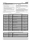
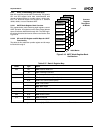
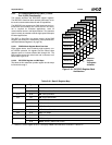
5.8.3.1 IR/SP3 Mode Register Bank Overview
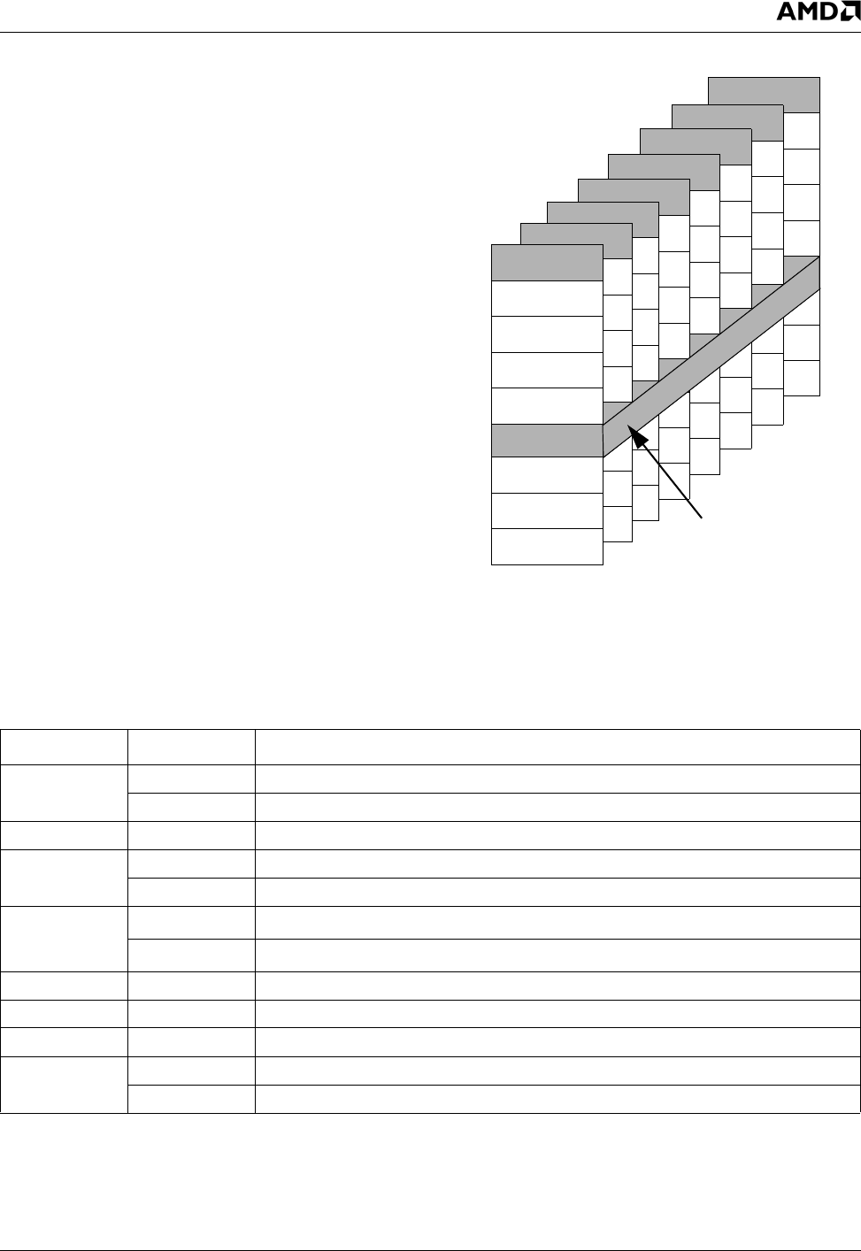
Eight register banks, each containing eight registers, con-
trol IR/SP3 operation. All registers use the same 8-byte
address space to indicate offsets 00h through 07h. The
BSR register selects the active bank and is common to all
banks. See Figure 5-19.
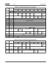
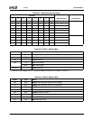
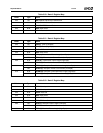
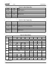
5.8.3.2 IRCP/SP3 Register and Bit Maps
The tables in this subsection provide register and bit maps
for Banks 0 through 7.
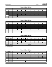
Figure 5-19. IRCP/SP3 Register Bank
Architecture
Bank 0
Bank 1
Bank 2
Bank 3
Bank 4
Bank 5
Bank 6
Bank 7
Offset 07h
Offset 06h
Offset 05h
Offset 04h
LCR/BSR
Offset 02h
Offset 01h
Offset 00h
Common
Register
Throughout
All Banks
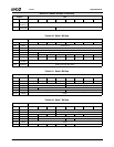
Table 5-46. Bank 0 Register Map
Offset Type Name
00h RO RXD. Receive Data Port
W TXD. Transmit Data Port
01h R/W IER. Interrupt Enable
02h RO EIR. Event Identification
R/W FCR. FIFO Control
03h W
LCR
1
. Link Control
R/W
BSR
1
. Bank Select
04h R/W MCR. Modem/Mode Control
05h R/W LSR. Link Status
06h R/W MSR. Modem Status
07h R/W SPR. Scratchpad
R/W ASCR. Auxiliary Status and Control
1. When bit 7 of this register is set to 1, bits [6:0] of BSR select the bank, as shown in Table 5-47.


