AMD Geode™ SC2200 Processor Data Book 205
Core Logic Module - Bridge, GPIO, and LPC Registers - Function 0
32580B
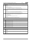
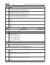
Index 52h ROM/AT Logic Control Register (R/W) Reset Value: 98h
7 Snoop Fast Keyboard Gate A20 and Fast Reset. Enables the snoop logic associated with keyboard commands for A20
Mask and Reset.
0: Disable snooping. The keyboard controller handles the commands.
1: Enable snooping.
6:5 Reserved. Must be set to 0.
4 Enable A20M# De-assertion on Warm Reset. Force A20M# high during a Warm Reset (guarantees that A20M# is de-
asserted regardless of the state of A20).
0: Disable.
1: Enable.
3 Enable Port 092h (Port A). Port 092h decode and the logical functions.
0: Disable.
1: Enable.
2 Upper ROM Size. Selects upper ROM addressing size.
0: 256K (FFFC0000h-FFFFFFFFh).
1: Use ROM Mask register (F0 Index 6Ch).
ROMCS# goes active for the above ranges whether strapped for ISA or LPC. (Refer to F0BAR1+I/O Offset 10h[15] for fur-
ther strapping/programming details.)
The selected range can then be either positively or subtractively decoded through F0 Index 5Bh[5].
1 ROM Write Enable. When asserted, enables writes to ROM space, allowing Flash programming.
If strapped for ISA and this bit is set to 1, writes to the configured ROM space asserts ROMCS#, enabling the write cycle to
the Flash device on the ISA bus. Otherwise, ROMCS# is inhibited for writes.
If strapped for LPC and this bit is set to 1, the cycle runs on the LPC bus. Otherwise, the LPC bus cycle is inhibited for
writes.
Refer to F0BAR1+I/O Offset 10h[15] for further strapping/programming details.
0 Lower ROM Size. Selects lower ROM addressing size in which ROMCS# goes active.
0: Lower ROM access are 000F0000h-000FFFFFh (64 KB). (Default)
1: Lower ROM accesses are 000E0000h-000FFFFFh (128 KB).
ROMCS# goes active for the above ranges whether strapped for ISA or LPC. (Refer to F0BAR1+I/O Offset 10h[15] for fur-
ther strapping/programming details.)
The selected range can then be either positively or subtractively decoded through F0 Index 5Bh[5].
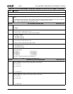
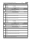
Index 53h Alternate CPU Support Register (R/W) Reset Value: 00h
7:6 Reserved. Must be set to 0.
5 Bidirectional SMI Enable.
0: Disable.
1: Enable.
This bit must be set to 0.
4:3 Reserved. Must be set to 0.
2 Reserved. Must be set to 0.
1 IRQ13 Function Selection. Selects function of the internal IRQ13/FERR# signal.
0: FERR#.
1: IRQ13.
This bit must be set to 1.
0 Generate SMI on A20M# Toggle.
0: Disable.
1: Enable.
This bit must be set to 1.
SMI status is reported at F1BAR0+I/O Offset 00h/02h[7].
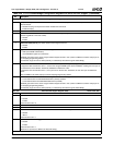
Index 54h-59h Reserved Reset Value: 00h
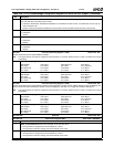
Table 6-29. F0: PCI Header/Bridge Configuration Registers for GPIO and LPC Support (Continued)
Bit Description


