


184 AMD Geode™ SC2200 Processor Data Book
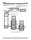
Core Logic Module - Register Summary
32580B
6.3.2 Register Summary
The tables in this subsection summarize the registers of
the Core Logic module. Included in the tables are the regis-
ter’s reset values and page references where the bit for-
mats are found.
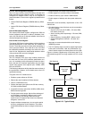
Note: Function 4 (F4) is for Video Processor support
(although accessed through the Core Logic PCI
configuration registers). Refer to Section 7.3.1
"Register Summary" on page 338 for details.
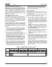
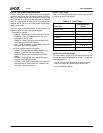
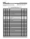
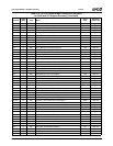
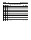
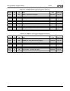
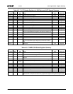
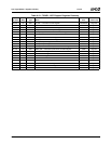
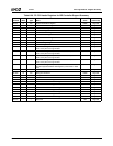
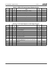
Table 6-14. F0: PCI Header/Bridge Configuration Registers
for GPIO and LPC Support Summary
F0 Index
Width
(Bits) Type Name
Reset
Value
Reference
(Table 6-29)
00h-01h 16 RO Vendor Identification Register 100Bh Page 198
02h-03h 16 RO Device Identification Register 0500h Page 198
04h-05h 16 R/W PCI Command Register 000Fh Page 198
06h-07h 16 R/W PCI Status Register 0280h Page 199
08h 8 RO Device Revision ID Register 00h Page 200
09h-0Bh 24 RO PCI Class Code Register 060100h Page 200
0Ch 8 R/W PCI Cache Line Size Register 00h Page 200
0Dh 8 R/W PCI Latency Timer Register 00h Page 200
0Eh 8 RO PCI Header Type Register 80h Page 200
0Fh 8 RO PCI BIST Register 00h Page 200
10h-13h 32 R/W Base Address Register 0 (F0BAR0) — Sets the base address for
the I/O mapped GPIO Runtime and Configuration Registers (sum-
marized in Table 6-15).
00000001h Page 200
14h-17h 32 R/W Base Address Register 1 (F0BAR1) — Sets the base address for
the I/O mapped LPC Configuration Registers (summarized in
Table 6-16)
00000001h Page 200
18h-2Bh --- --- Reserved 00h Page 200
2Ch-2Dh 16 RO Subsystem Vendor ID 100Bh Page 200
2Eh-2Fh 16 RO Subsystem ID 0500h Page 200
30h-3Fh --- --- Reserved 00h Page 200
40h 8 R/W PCI Function Control Register 1 39h Page 201
41h 8 R/W PCI Function Control Register 2 00h Page 201
42h --- --- Reserved 00h Page 202
43h 8 R/W PIT Delayed Transactions Register 02h Page 202
44h 8 R/W Reset Control Register 01h Page 203
45h --- --- Reserved 00h Page 203
46h 8 R/W PCI Functions Enable Register FEh Page 203
47h 8 R/W Miscellaneous Enable Register 00h Page 204
48h-4Bh --- --- Reserved 00h Page 204
4Ch-4Fh 32 R/W Top of System Memory FFFFFFFFh Page 204
50h 8 R/W PIT Control/ISA CLK Divider 7Bh Page 204
51h 8 R/W ISA I/O Recovery Control Register 40h Page 205
52h 8 R/W ROM/AT Logic Control Register 98h Page 205
53h 8 R/W Alternate CPU Support Register 00h Page 206
54h-59h --- --- Reserved 00h Page 206
5Ah 8 R/W Decode Control Register 1 01h Page 206
5Bh 8 R/W Decode Control Register 2 20h Page 207
5Ch 8 R/W PCI Interrupt Steering Register 1 00h Page 208
5Dh 8 R/W PCI Interrupt Steering Register 2 00h Page 208
5Eh-5Fh --- --- Reserved 00h Page 208
60h-63h 32 R/W ACPI Control Register 00000000h Page 208
64h-6Bh --- --- Reserved 00h Page 209