


298 AMD Geode™ SC2200 Processor Data Book
Core Logic Module - USB Controller Registers - PCIUSB
32580B
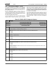
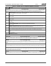
Offset 34h-37h HcFmInterval Register (R/W) Reset Value = 00002EDFh
31 FrameIntervalToggle (Read Only). This bit is toggled by HCD when it loads a new value into FrameInterval.
30:16 FSLargestDataPacket (Read Only). This field specifies a value which is loaded into the Largest Data Packet Counter at
the beginning of each frame.
15:14 Reserved. Read/Write 0s.
13:0 FrameInterval. This field specifies the length of a frame as (bit times - 1). For 12,000 bit times in a frame, a value of 11,999
is stored here.
Offset 38h-3Bh HcFrameRemaining Register (RO) Reset Value = 00000000h
31 FrameRemainingToggle (Read Only). Loaded with FrameIntervalToggle when FrameRemaining is loaded.
30:14 Reserved. Read 0s.
13:0 FrameRemaining (Read Only). When the HC is in the UsbOperational state, this 14-bit field decrements each 12 MHz
clock period. When the count reaches 0, (end of frame) the counter reloads with FrameInterval. In addition, the counter
loads when the HC transitions into UsbOperational.
Offset 3Ch-3Fh HcFmNumber Register (RO) Reset Value = 00000000h
31:16 Reserved. Read 0s.
15:0 FrameNumber (Read Only). This 16-bit incrementing counter field is incremented coincident with the loading of FrameR-
emaining. The count rolls over from FFFFh to 0h.
Offset 40h-43h HcPeriodicStart Register (R/W) Reset Value = 00000000h
31:14 Reserved. Read/Write 0s.
13:0 PeriodicStart. This field contains a value used by the List Processor to determine where in a frame the Periodic List pro-
cessing must begin.
Offset 44h-47h HcLSThreshold Register (R/W) Reset Value = 00000628h
31:12 Reserved. Read/Write 0s.
11:0 LSThreshold. This field contains a value used by the Frame Management block to determine whether or not a low speed
transaction can be started in the current frame.
Offset 48h-4Bh HcRhDescriptorA Register (R/W) Reset Value = 01000003h
31:24 PowerOnToPowerGoodTime. This field value is represented as the number of 2 ms intervals, ensuring that the power
switching is effective within 2 ms. Only bits [25:24] are implemented as R/W. The remaining bits are read only as 0. It is not
expected that these bits be written to anything other than 1h, but limited adjustment is provided. This field should be written
to support system implementation. This field should always be written to a non-zero value.
23:13 Reserved. Read/Write 0s.
12 NoOverCurrentProtection. This bit should be written to support the external system port over-current implementation.
0: Over-current status is reported.
1: Over-current status is not reported.
11 OverCurrentProtectionMode. This bit should be written 0 and is only valid when NoOverCurrentProtection is cleared.
0: Global Over-Current.
1: Individual Over-Current.
10 DeviceType (Read Only). USB is not a compound device.
9 NoPowerSwitching. This bit should be written to support the external system port power switching implementation.
0: Ports are power switched.
1: Ports are always powered on.
8
PowerSwitchingMode. This bit is only valid when NoPowerSwitching is cleared. This bit should be written 0.
0: Global Switching.
1: Individual Switching.
Table 6-42. USB_BAR+Memory Offset: USB Controller Registers (Continued)
Bit Description