


132 AMD Geode™ SC2200 Processor Data Book
SuperI/O Module
32580B
5.7.10 ACB Registers
Each functional block is associated with a Logical Device
Number (LDN) (see Section 5.3.2 "Banked Logical Device
Registers" on page 98). ACCESS.Bus Port 1 is assigned
as LDN 05h and ACCESS.bus Port 2 as LDN 06h. In addi-
tion to the registers listed here, there are additional config-
uration registers listed in Section 5.4.2.5 "LDN 05h and 06h
- ACCESS.bus Ports 1 and 2" on page 109.
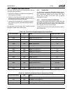
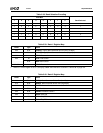
Table 5-31. ACB Register Map
Offset Type Name
Reset
Value
00h R/W ACBSDA. ACB Serial Data xxh
01h R/W ACBST. ACB Status 00h
02h R/W ACBCST. ACB Control Status 00h
03h R/W ACBCTL1. ACB Control 1 00h
04h R/W ACBADDR. ACB Own Address xxh
05h R/W ACBCTL2. ACB Control 2 00h
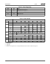
Table 5-32. ACB Registers
Bit Description
Offset 00h ACB Serial Data Register - ACBSDA (R/W) Reset Value: xxh
7:0 ACB Serial Data. This shift register is used to transmit and receive data. The most significant bit is transmitted (received)
first, and the least significant bit is transmitted last. Reading or writing to ACBSDA is allowed only when ACBST[6] is set, or
for repeated starts after setting the ACBCTL1[0]. An attempt to access the register in other cases may produce unpredict-
able results.
Offset 01h ACB Status Register - ACBST (R/W) Reset Value: 00h
This is a read register with a special clear. Some of its bits may be cleared by software, as described below. This register maintains the
current ACB status. On reset, and when the ACB is disabled, ACBST is cleared (00h).
7 SLVSTP (Slave Stop). (R/W1C) Writing 0 to SLVSTP is ignored.
0: Writing 1 or ACB disabled.
1: Stop Condition detected after a slave transfer in which ACBCST[2] or ACBCST[3] was set.
6 SDAST (SDA Status). (RO)
0: Reading from ACBSDA during a receive, or when writing to it during a transmit. When ACBCTL1[0] is set, reading ACB-
SDA does not clear SDAST. This enables ACB to send a repeated start in master receive mode.
1: SDA Data Register awaiting data (transmit - master or slave) or holds data that should be read (receive - master or
slave).
5 BER (Bus Error). (R/W1C) Writing 0 to this bit is ignored.
0: Writing 1 or ACB disabled.
1: Start or Stop Condition detected during data transfer (i.e., Start or Stop Condition during the transfer of bits [8:2] and
acknowledge cycle), or when an arbitration problem detected.
4 NEGACK (Negative Acknowledge). (R/W1C) Writing 0 to this bit is ignored.
0: Writing 1 or ACB disabled.
1: Transmission not acknowledged on the ninth clock (In this case, SDAST (bit 6) is not set).
3 STASTR (Stall After Start). (R/W1C) Writing 0 to this bit is ignored.
0: Writing 1 or ACB disabled.
1: Address sent successfully (i.e., a Start Condition sent without a bus error, or Negative Acknowledge), if ACBCTL1[7] is
set. This bit is ignored in slave mode. When STASTR is set, it stalls the ACCESS.bus by pulling down the ABC line, and
suspends any further action on the bus (e.g., receive of first byte in master receive mode). In addition, if ACBCTL1[1] is
set, it also causes the ACB to send an interrupt.
2 NMATCH (New Match). (R/W1C) Writing 0 to this bit is ignored. If ACBCTL1[2] is set, an interrupt is sent when this bit is
set.
0: Software writes 1 to this bit.
1: Address byte follows a Start Condition or a repeated start, causing a match or a global-call match.