


193
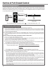
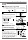
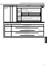
[Connection and Setup of Full-closed Control]
Full-Closed
Control Mode
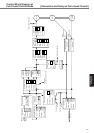
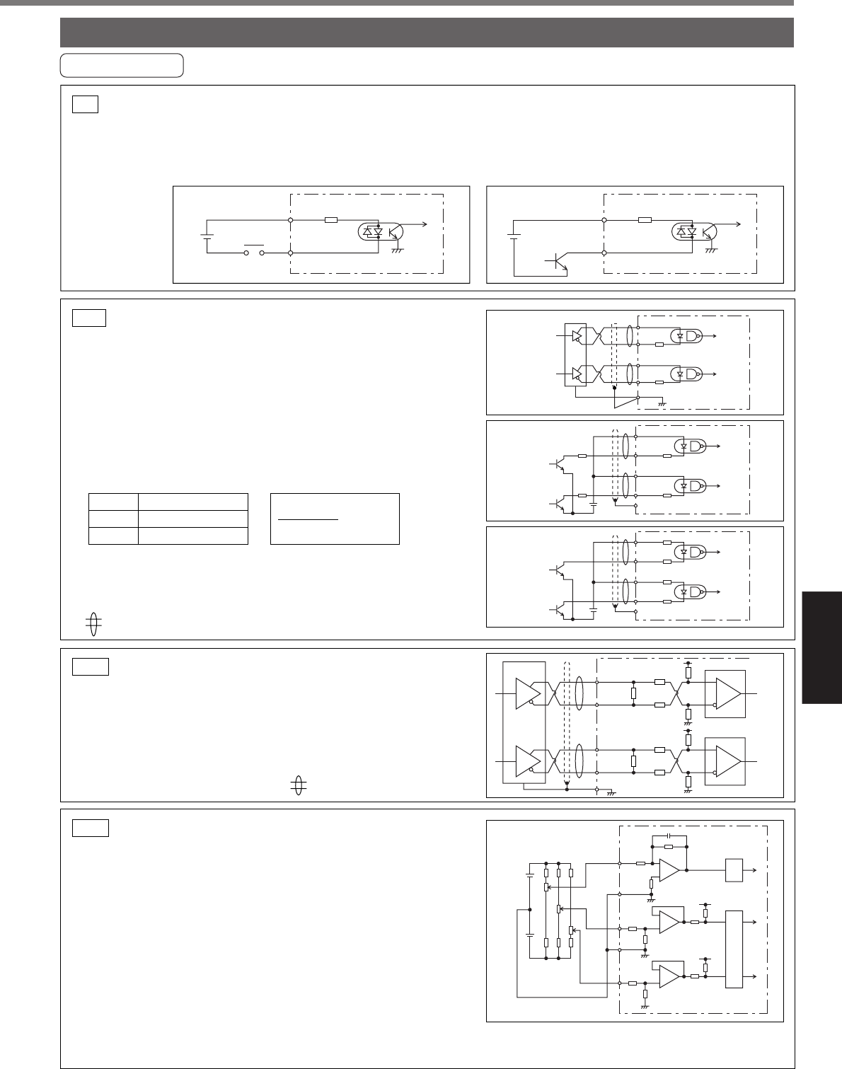
Interface Circuit
Input Circuit
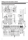
(1) Line driver I/F (Input pulse frequency : max. 500kpps)
• This signal transmission method has better noise immunity.
We recommend this to secure the signal transmission.
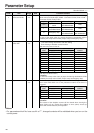
(2)Open collector I/F (Input pulse frequency : max. 200kpps)
•
The method which uses an external control signal power supply (VDC)
• Current regulating resistor R corresponding to V
DC
is
required in this case.
• Connect the specified resister as below.
(3)Open collector I/F (Input pulse frequency : max. 200kpps)
• Connecting diagram when a current regulating resistor is not
used with 24V power supply.
Connection to sequence input signals (Pulse train interface)
PI1
Max.input voltage : DC24V,
Rated current : 10mA
V
DC
12V
24V
Specifications
1kΩ1/2W
2kΩ1/2W
V
DC
–1.5
R+220
.
=
.
10mA
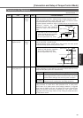
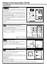
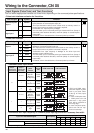
Line driver I/F (Input pulse frequency : max. 2Mpps)
• This signal transmission method has better noise immunity.
We recommend this to secure the signal transmission
when line driver I/F is used.
Connection to sequence input signals
(Pulse train interface exclusive to line driver)
PI2
AM26LS31 or equivalent
3
PULS1
H/L
ON/OFF
ON/OFF
H/L
H/L
PULS
L/H
PULS
L/H
SIGN
H/L
SIGN
PULS2
SIGN1
SIGN2
GND
220Ω
220Ω
4
5
6
13
PULS1
PULS2
SIGN1
GND
SIGN2
220Ω
220Ω
V
DC
R
R
3
4
5
6
13
(1)
(2)
ON/OFF
ON/OFF
L/H
PULS
L/H
SIGN
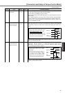
OPC1
PULS2
OPC2
GND
SIGN2
220Ω
220Ω
2.2kΩ
2.2kΩ
V
DC
1
4
2
6
13
(3)
represents twisted pair.
represents twisted pair.
• Connect to contacts of switches and relays, or open collector output transistors.
• When you use contact inputs, use the switches and relays for micro current to avoid contact failure.
• Make the lower limit voltage of the power supply (12 to 24V) as 11.4V or more in order to secure the primary
current for photo-couplers.
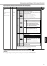
Connection to sequence input signalsSI
12 to 24V
7 COM+4.7kΩ
SRV-ON etc.
Relay
7 COM+4.7kΩ
12 to 24V
SRV-ON etc.
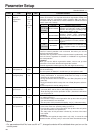
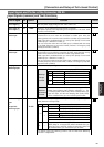
Analog command input
AI
• The analog command input goes through 3 routes,
SPR/TRQR(Pin-14), CCWTL (Pin-16) and CWTL (Pin-18).
• Max. permissible input voltage to each input is ±10V.
For input impedance of each input, refer to the right Fig.
• When you compose a simple command circuit using variable
resistor(VR) and register R, connect as the right Fig. shows.
When the variable range of each input is made as –10V to
+10V, use VR with 2kΩ, B-characteristics, 1/2W or larger, R
with 200Ω, 1/2W or larger.
• A/D converter resolution of each command input is as follows.
(1)ADC1 : 16 bit (SPR/TRQR), (including 1bit for sign), ±10V
(2)ADC2 : 10 bit (CCWTL, CWTL), 0 – 3.3V
+12V
+3.3V
SPR/TRQR
CCWTL
CWTL
R
14
20kΩ
20kΩ
1kΩ
1kΩ
10kΩ
GND
GND
10kΩ
3.83kΩ
3.83kΩ
ADC
1
ADC
2
15
16
17
18
R
VR
–12V
+
–
+
–
+
–
+3.3V
1kΩ
1kΩ
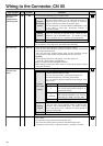
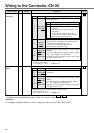
44
45
13
2kΩ
43kΩ
43kΩ
2kΩ
220Ω
GND
H/L
H/L
PULS
SIGN
AM26C32 or equivalent
46
47
2kΩ
43kΩ
43kΩ
2kΩ
220Ω
H/L
H/L
PULS
SIGN
AM26C32 or equivalent