


Timers
16-Bit Timer Setup Examples
Panasonic Semiconductor Development Company MN102H75K/F75K/85K/F85K LSI User Manual
102
Panasonic
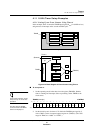
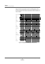
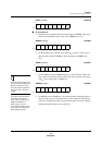
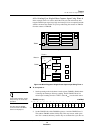
P2DIR (example) x’00FFE2’
■ To set up timer 0:
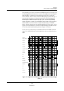
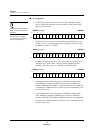
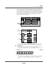
1. Disable timer 0 counting in the timer 0 mode register (TM0MD). This step is
unnecessary immediately after a reset, since TM0MD resets to 0.
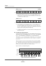
TM0MD (example) x’00FE20’
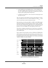
2. Set the divide-by ratio for timer 0. To divide B
OSC
/4 by two, write x’01’ to
the timer 0 base register (TM0BR). (The valid range for TM0BR is 0 to
255.)
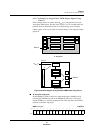
TM0BR (example) x’00FE10’
Do not change the clock source
once you select it. Selecting the
clock source while you set up
the count operation control will
corrupt the value in the binary
counter.
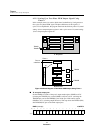
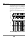
3. Set the TM0LD bit of the TM0MD register to 1. This loads the value in the
base register to the binary counter. At the same time, select the clock source
as B
OSC
/4 by writing b’00’ to TM0S[1:0].
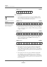
TM0MD (example) x’00FE20’
In the bank and linear address-
ing versions of the MN102
series, it was necessary to set
TM0EN and TM0LD to 0
between steps 3 and 4, to
ensure stable operation. This is
unnecessary in the high-speed
linear addressing version.
4. Set TM0LD to 0 and TM0EN to 1. This starts the timer. Counting begins at
the start of the next cycle. When the binary counter reaches 0 and loads the
value x’01’ from the base register, in preparation for the next count, a timer 0
underflow interrupt request is sent to the CPU.
Bit:76543210
P2
DIR7
P2
DIR6
P2
DIR5
P2
DIR4
P2
DIR3
P2
DIR2
P2
DIR1
P2
DIR0
Setting:01100000
Bit:76543210
TM0
EN
TM0
LD
————
TM0
S1
TM0
S0
Setting:000000——
Bit:76543210
TM0
BR7
TM0
BR6
TM0
BR5
TM0
BR4
TM0
BR3
TM0
BR2
TM0
BR1
TM0
BR0
Setting:00000001
Bit:76543210
TM0
EN
TM0
LD
————
TM0
S1
TM0
S0
Setting:01000000