


On-Screen Display
OSD Registers
MN102H75K/F75K/85K/F85K LSI User Manual Panasonic Semiconductor Development Company
203
Panasonic
7.15 OSD Registers
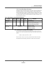
All registers in OSD block cannot be written by byte (by word only). Read by
byte is possible.
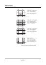
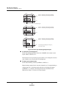
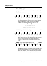
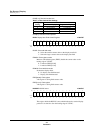
CROMEND: Text ROM End Address Register x’007F00’
A[17:8] holds the programmable portion of the text ROM end address. The
low-order 8 bits of the address are always x’FF’ and the high-order 6 bits
are always b’000010’. The available address range is x’0800FF’ to
x’0BFFFF’, with a programmable range from x’000’ to x’3FF’.
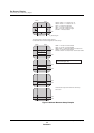
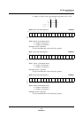
GROMEND: Graphics ROM End Address Register x’007F02’
A[17:8] holds the programmable portion of the graphics ROM end
address. The low-order 8 bits of the address are always x’FF’ and the high-
order 6 bits are always b’000010’. The available address range is
x’0800FF’ to x’0BFFFF’, with a programmable range from x’000’ to
x’3FF’.
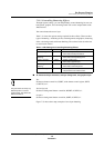
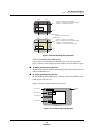
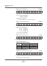
RAMEND: Text and Graphics RAM End Address Register x’007F04’
GRAMENDA[11:4] holds the programmable portion of the graphics RAM
end address and CRAMENDA[11:4] holds the programmable portion of
the text RAM end address. The low-order 4 bits of the address are always
x’F’ and the high-order 4 bits are always x’9’. The available address range
Bit:1514131211109876543210
——————A17A16A15A14A13A12A11A10A9A8
Reset:0000000000000000
R/W:RRRRRRR/WR/WR/WR/WR/WR/WR/WR/WR/WR/W
Bit:1514131211109876543210
——————A17A16A15A14A13A12A11A10A9A8
Reset:0000000000000000
R/W:RRRRRRR/WR/WR/WR/WR/WR/WR/WR/WR/WR/W
Bit:1514131211109876543210
GRAM
END
A11
GRAM
END
A10
GRAM
END
A9
GRAM
END
A8
GRAM
END
A7
GRAM
END
A6
GRAM
END
A5
GRAM
END
A4
CRAM
END
A11
CRAM
END
A10
CRAM
END
A9
CRAM
END
A8
CRAM
END
A7
CRAM
END
A6
CRAM
END
A5
CRAM
END
A4
Reset:0000000000000000
R/W: R/W R/W R/W R/W R/W R/W R/W R/W R/W R/W R/W R/W R/W R/W R/W R/W
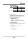
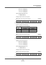
0000 10XX XXXX XXXX 1111 1111
0000 1000 0000 0000 1111 1111
0000 1011 1111 1111 1111 1111
Fixed Programmable Fixed
0800FF
0BFFFF
A17 A8