


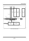
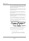
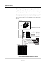
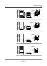

On-Screen Display
VRAM
MN102H75K/F75K/85K/F85K LSI User Manual Panasonic Semiconductor Development Company
169
Panasonic
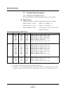
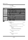
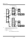
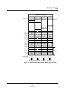
7.8.2 VRAM Organization
Notes: 1. All addresses are expressed in hex notation. Other values are decimal.
2. GRAMEND: Graphics RAM end address (programmable to any address)
3. CRAMEND: Text RAM end address (programmable to any address)
4. M: Number of lines in the text layer
5. m: 1 and up
6. N: Number of lines in the graphics layer
7. n: 1 and up
Figure 7-6 VRAM Organization (When GEXTE = 0)
GRAMEND−3F
GRAMEND−3E
GRAMEND−3D
GRAMEND−3C
GRAMEND−3B
GRAMEND−3A
GRAMEND−2F
GRAMEND−2E
GRAMEND−3
GRAMEND−2
GRAMEND−1
GRAMEND
Unused area
Unused area
Code 30
Code 29
.
.
.
Code 2
Code 1
2 bytes
Low-order 8 bits
of graphics code
High-order 8 bits
of graphics code
GRAMEND−40×N+5
GRAMEND−40×(N−1)
GRAMEND−40×n+5
GRAMEND−40×(n−1)
GRAMEND−7B
GRAMEND−40
GRAMEND−3B
GRAMEND
Line N data
.
.
.
Line n data
.
.
.
Line 2 data
Line 1 data
64 bytes
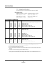
Graphics RAM Addresses
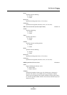
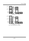
(When GEXTE = 1)
CRAMEND−4F
CRAMEND−4E
CRAMEND−4D
CRAMEND−4C
CRAMEND−4B
CRAMEND−4A
CRAMEND−3
CRAMEND−2
CRAMEND−1
CRAMEND
Code 40
Code 39
Code 38
.
.
.
Code 2
Code 1
2 bytes
Low-order 8 bits
of text code
High-order 8 bits
of text code
CRAMEND−50×M+1
CRAMEND−50×(M−1)
CRAMEND−50×m+1
CRAMEND−50×(m−1)
CRAMEND−9F
CRAMEND−50
CRAMEND−4F
CRAMEND
Line M data
.
.
.
Line m data
.
.
.
Line 2 data
Line 1 data
80 bytes
Text RAM Addresses
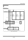
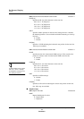
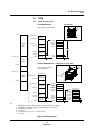
GRAMEND−40×N+5
GRAMEND
CRAMEND−50×M+1
CRAMEND
Program
Data
and
Stack
Area
Graphics
VRAM
Text
VRAM
x'009FFF'
x'008000'