


Closed-Caption Decoder
Closed-Caption Decoder Registers
Panasonic Semiconductor Development Company MN102H75K/F75K/85K/F85K LSI User Manual
242
Panasonic
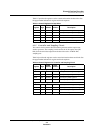
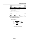
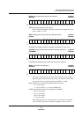
DATAE: Data Capture Stop Timing Control Register x’007E1A’
(DATAEW x’007E3A’)
DATAE[10:0]: Stop position for data capture
Set this value high enough to allow the last data to be captured. The valid
range is x’000’ to x’7FF’.
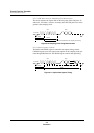
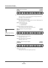
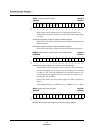
STAP: Sampling Start Position Register (Software Setting) x’007E1C’
(STAPW x’007E3C’)
SFTSTAP[10:0]: Software setting for sampling start position (in clock units)
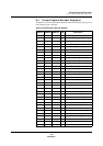
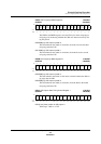
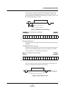
FCPNUM: Sampling Start Position Register (Hardware Calculation) x’007E1E’
(FCPNUMW x’007E3E’)
FCPNUM[10:0]: Sampling start position calculated by the hardware
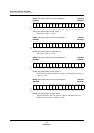
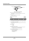
NFSEL: Noise Filter Select Register x’007EC0’
(NFSELW x’007EE0’)
This register selects the low-pass filter, which eliminates noise and high-
frequency signals that are unnecessary to the sync separator and the clamp-
ing controller. The recommended setting for NFSEL is x’0000’.
MING: Output select for noise filter detecting minimum sync tip
0: Low-pass filter 1
1: Low-pass filter 2, 3, or 4 (set in NFSW[1:0])
NFSW[1:0]: Noise filter switch (for composite sync separator)
00: Low-pass filter 3
01: Low-pass filter 4
10: Low-pass filter 2
11: Low-pass filter 1
The cutoff frequencies for low-pass filters 1 to 4 are lower in ascending
order, so that low-pass filter 4 eliminates the highest amount of noise.
Bit:1514131211109876543210
—————
DATA
E
10
DATA
E
9
DATA
E
8
DATA
E
7
DATA
E
6
DATA
E
5
DATA
E
4
DATA
E
3
DATA
E
2
DATA
E
1
DATA
E
0
Reset:0000011111111111
R/W:RRRRRR/WR/WR/WR/WR/WR/WR/WR/WR/WR/WR/W
Bit:1514131211109876543210
—————
SFT
STAP
10
SFT
STAP
9
SFT
STAP
8
SFT
STAP
7
SFT
STAP
6
SFT
STAP
5
SFT
STAP
4
SFT
STAP
3
SFT
STAP
2
SFT
STAP
1
SFT
STAP
0
Reset:0000011111111111
R/W:RRRRRR/WR/WR/WR/WR/WR/WR/WR/WR/WR/WR/W
Bit:1514131211109876543210
—————
FCP
NUM
10
FCP
NUM
9
FCP
NUM
8
FCP
NUM
7
FCP
NUM
6
FCP
NUM
5
FCP
NUM
4
FCP
NUM
3
FCP
NUM
2
FCP
NUM
1
FCP
NUM
0
Reset:0000000000000000
R/W:RRRRRRRRRRRRRRRR
Bit:1514131211109876543210
———————MING——————
NFSW
1
NFSW
0
Reset:0000000000000000
R/W:RRRRRRRR/WRRRRRRR/WR/W