


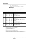

On-Screen Display
VRAM
MN102H75K/F75K/85K/F85K LSI User Manual Panasonic Semiconductor Development Company
171
Panasonic
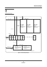
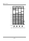
7.8.3 Cautions about the number of display code set to VRAM
When the display lines are adjoined or overlapped, and the number of the above
display code is extremely fewer than that of the below one, first line of the
display line may not be output correctly.
In OSD circuit, font data to display are read from ROM and stored to the buffer.
The data in the buffer are overwritten, after the present display code is output, to
the display data of the next line.
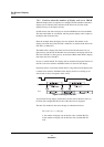
Show the example when the display lines are adjoined. The number of the
display code in the above line (line M) is reffered to n, and that of the below one
(line M+1) is refferred N.
The buffer holds n display data of the last line of line M at the time of A (see
figure below), and the data in the buffer are overwritten to the display data of the
first line of line M+1 as time goes by. At the time of B the buffer holds n display
data of the first line of line M+1.
In case n is smaller than N, N-n display data are needed to display the first line of
line M+1, and to be written to the buffer before it is shown on the display.
Especially when n is extremely smaller than N, a large amount of the display data
is needed to be written to the buffer before display. And in case writing is not
done in time, it shows wrong data on the screen.
To prevent the wrong display written above, the first line of the below line is to
be shown later enough after the last line of the above line is displayed.
The time (Td) needed for the correct display is caluculated as below.
Td = 0.8 + ( N - n )
× 0.5 [µs]
n : the number of display code in the above line. (include HP, VP)
N: the number of display code in the below line. (include HP, VP)
n<N
Figure 7-8 Timing for OSD data
HSYNC
display
Buffer
CBA