


I/O Ports
I/O Port Control Registers
MN102H75K/F75K/85K/F85K LSI User Manual Panasonic Semiconductor Development Company
277
Panasonic
11.3 I/O Port Control Registers
Do not activate the pullup resis-
tors when the pins are in output
mode. This will cause incorrect
output voltage levels and
increase power and current con-
sumption.
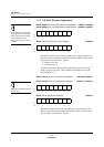
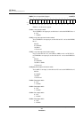
P0PUP–P5PUP: Ports 0–5 Pullup Resistor Control Registers x’00FFB0’–x’00FFB5’
P7PUP–P8PUP: Ports 7–8 Pullup Resistor Control Registers x’00FFB8’–x’00FFBA’
P6PUP: Port 6 Pullup Resistor Control Register x’00FFB6’
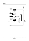
The PnPUP registers control the port pullup resistors. The bit number cor-
responds to the associated pin number. For instance, P0PUP7 applies to the
P07 pin. These are 8-bit access registers.
0: Pullup resistor off
1: Pullup resistor on
Note that by default the P7P8CNT bit of the PCNT2 register forces the
pullup resistors on for ports 7 and 8. P7PUP and P8PUP are only valid
when P7P8CNT is 1.
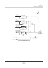
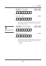
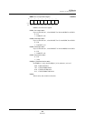
P0OUT–P5OUT: Ports 0–5 Output Control Registers x’00FFC0’–x’00FFC5’
Writing a 0 to P5OUT3 causes a
reset to occur.
P7OUT–P8OUT: Ports 7–8 Output Control Registers x’00FFC8’–x’00FFCA’
P6OUT: Port 6 Output Control Register x’00FFC6’
The PnOUT registers contain the port output data. The bit number corre-
sponds to the associated pin number. For instance, P0OUT7 applies to the
P07 pin. These are 8-bit access registers.
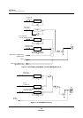
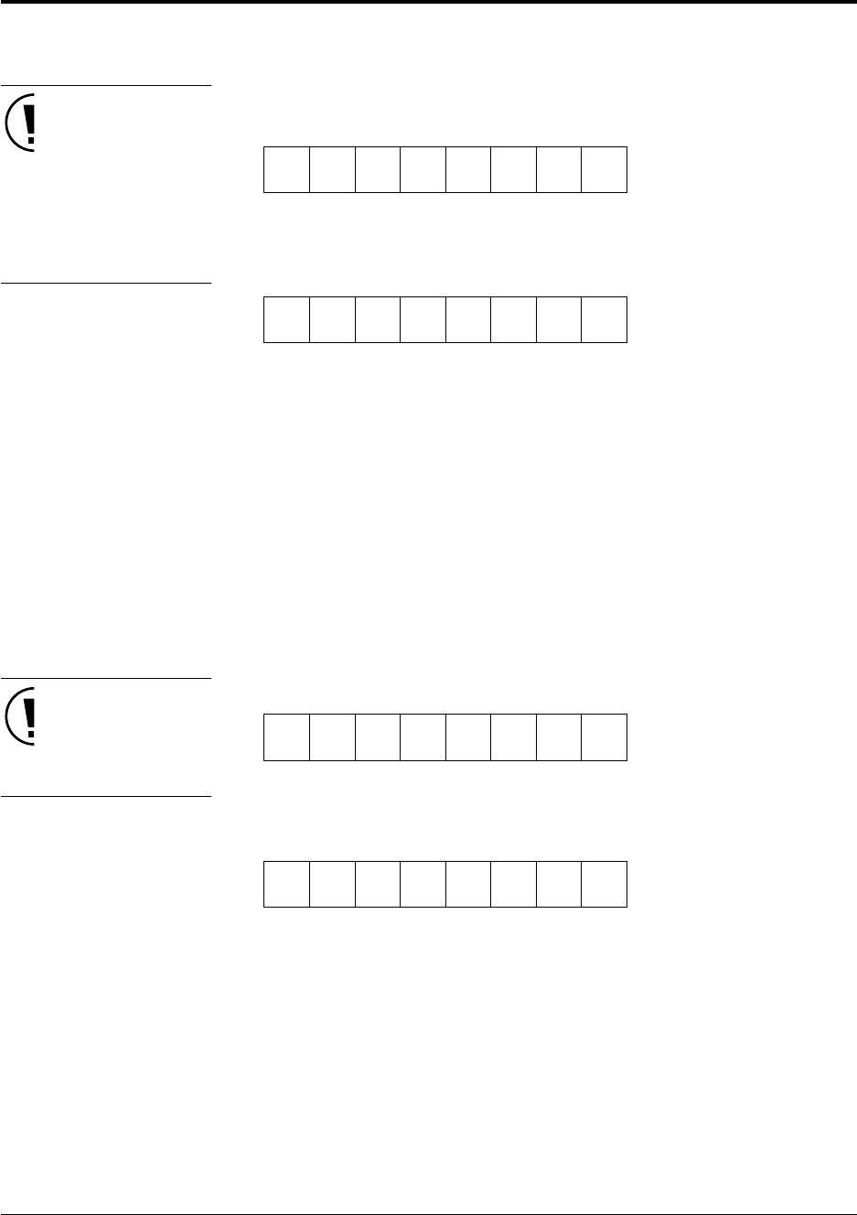
Bit:76543210
PnPUP7 PnPUP6 PnPUP5 PnPUP4 PnPUP3 PnPUP2 PnPUP1 PnPUP0
Reset:00000000
R/W: R/W R/W R/W R/W R/W R/W R/W R/W
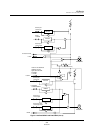
Bit:76543210
000000P6PUP1P6PUP0
Reset:00000000
R/W:RRRRRRR/WR/W
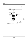
Bit:76543210
PnOUT7 PnOUT6 PnOUT5 PnOUT4 PnOUT3 PnOUT2 PnOUT1 PnOUT0
Reset:00000000
R/W: R/W R/W R/W R/W R/W R/W R/W R/W
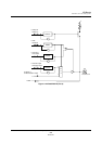
Bit:76543210
000000P6OUT1P6OUT0
Reset:00000000
R/W:RRRRRRR/WR/W