


On-Screen Display
Selecting the OSD Dot Clock
MN102H75K/F75K/85K/F85K LSI User Manual Panasonic Semiconductor Development Company
193
Panasonic
7.12 Selecting the OSD Dot Clock
This section describes how to set up the OSD dot clock.
■
Selecting the clock source
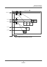
The source for the OSD dot clock is programmable to either the 4-MHz clock
supplied through the OSC1 and OSC2 pins, then multiplied by the PLL circuit to
48 MHz, or a dedicated clock supplied through the OSDXI and OSDXO pins.
The dedicated OSDX clock can be a crystal, LC oscillator, or other form of exci-
tation that is input through the OSDXI pin and synchronized internally to the
HSYNC pulse, or it can be an LC blocking oscillator synchronized to the
HSYNC pulse.
If your design uses the OSDX clock, set the XIO bit (x’007F06’, bit 7) for the
appropriate frequency.
♦ XIO
0: Less than 20 MHz
1: Greater than 20 MHz
■
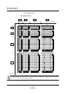
Selecting the divide-by ratio
There are five divide-by settings available for any of the clocks described above.
Table 7-11 shows the register settings for each ratio.
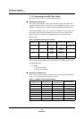
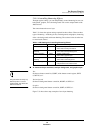
Table 7-10 OSD Dot Clock Source Settings
OSCSEL1
(x’007F06’, bit 9)
OSCSEL0
(x’007F06’, bit 8)
Oscillator pins Oscillator type Frequency
0 0 OSC1, OSC2 Crystal + PLL 48-MHz
(with 4-MHz osc.)
01OSDXI,
OSDXO
LC blocking
oscillator
f
X
10OSDXI,
OSDXO
Crystal, LC
oscillator, or
other excitation
f
X
1 1 Reserved — —
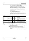
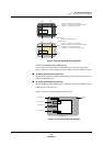
Table 7-11 OSD Dot Clock Division Settings
VCLK2
(x’007F08’, bit 6)
VCLK1
(x’007F08’, bit 5)
VCLK0
(x’007F08’, bit 4)
Divide by Ratio
0 0 0 1/4 (12 MHz)
(1)
0 0 1 1/3 (16 MHz)
(1)
0 1 0 1/2 (24 MHz)
(1)
0 1 1 2/3 (32 MHz)
(1)
1 0 0 1/1 (48 MHz)
1 0 1 Reserved
1 1 0 Reserved
1 1 1 Reserved
Notes: 1. This is the frequency with a 48-MHz clock source.