


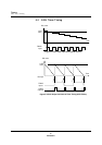
Timers
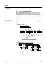
8-Bit Timer Setup Examples
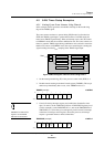
MN102H75K/F75K/85K/F85K LSI User Manual Panasonic Semiconductor Development Company
85
Panasonic
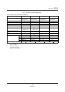
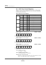
TM2UDICH (example) x’00FC71’
TM2UDICL (example) x’00FC70’
TM1UDICH (example) x’00FC73’
TM1UDICL (example) x’00FC72’
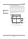
3. Set the divide-by ratio for timer 0. Since the timer will count 60,000 cycles
(x’EA60’), write x’5F’ to the timer 1 base register (TM1BR) and x’EA’ to
the timer 2 base register (TM2BR). (The valid range for TMnBR is 0 to
255.)
TM1BR (example) x’00FE11’
TM2BR (example) x’00FE12’
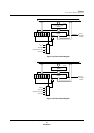
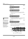
Do not change the clock source
once you select it. Selecting the
clock source while you set up
the count operation control will
corrupt the value in the binary
counter.
4. Set the TM1LD bit of the TM1MD register and theTM2LD bit of the
TM2MD register to 1. This loads the value in the base register to the binary
counter. At the same time, select the clock source as the BOSC/4 for timer 1
and cascade to timer 1 for timer 2. (Write to TMnS[1:0]).
TM1MD (example) x’00FE21’
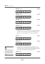
Bit:76543210
—
TM2UD
LV 2
TM2UD
LV 1
TM2UD
LV 0
———
TM2UD
IE
Setting:01000001
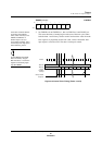
Bit:76543210
———
TM2UD
IR
———
TM2UD
ID
Setting:00000000
Bit:76543210
———————
TM0UD
IE
Setting:00000000
Bit:76543210
———
TM1UD
IR
———
TM1UD
ID
Setting:00000000
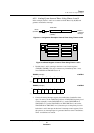
Bit:76543210
TM1
BR7
TM1
BR6
TM1
BR5
TM1
BR4
TM1
BR3
TM1
BR2
TM1
BR1
TM1
BR0
Setting:01011111
Bit:76543210
TM2
BR7
TM2
BR6
TM2
BR5
TM2
BR4
TM2
BR3
TM2
BR2
TM2
BR1
TM2
BR0
Setting:11101010
Bit:76543210
TM1
EN
TM1
LD
————
TM1
S1
TM1
S0
Setting:01000000