


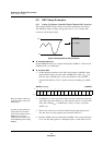

On-Screen Display
Power-Saving Considerations in the OSD Block
MN102H75K/F75K/85K/F85K LSI User Manual Panasonic Semiconductor Development Company
155
Panasonic
7.4 Power-Saving Considerations in the OSD
Block
Table 7-2 shows bits that can decrease the power consumption of the OSD block.
This section explains how to use these bits.
OSDPOFF resets to 0. To
operate the OSD, you must first
set this bit to 1.
To turn off the OSD block to save
power:
1. Write a 0 to OSD (OSD1, bit 10).
2. Wait for the next VSYNC input.
3. Write a 0 to OSDPOFF (PCNT0,
bit 7), turning the clock off.
If you turn the clock off before the
VSYNC input, power usage may
not drop or the microcontroller may
halt.
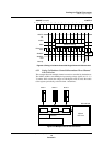
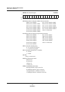
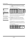
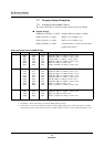
Table 7-2 Power-Saving Control Bits for the OSD
Using OSDPOFF to control the system clock supply to the OSD
The OSDPOFF bit enables or disables the system clock supply to the OSD block.
When the OSD is unused, setting this bit to 0 stops the clock supply to the OSD,
reducing power dissipation. Setting OSDPOFF to 0 not only disables the OSD
display, it disables reads from and writes to the OSD registers. To operate the
OSD, set this bit to 1, then set up the OSD registers.
Using OSDREGE to control read/write access to the OSD registers
The OSDREGE bit enables or disables read/write operations to the OSD reg-
isters. Once you have set the OSD registers, you can write a 0 to this bit to
disable furthers reads and writes to them, reducing power dissipation. This bit
resets to 0.
Note that when OSDPOFF is 0, you cannot read or write to the OSD registers
even if OSDREGE is 1. Table 7-3 shows the combinations of OSDPOFF and
OSDREGE. Note also that when OSDREGE is 0, the OSD display runs, but the
shuttering motion does not work. If your application requires shutter movement,
you must enable OSDREGE.
Bit Name Register Address Bit Description Reset
OSDPOFF PCNT0 x’00FF90’ 7 0: System clock off to OSD
1: System clock on to OSD
0
OSDREG
E
PCNT2 x’00FF92’ 0 0: R/W disabled for OSD registers
1: R/W enabled for OSD registers
0
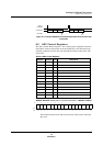
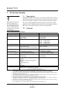
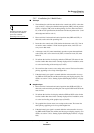
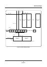
Table 7-3 OSDPOFF and OSDREGE Settings
OSDPOFF OSDREGE OSD Register R/W Power Dissipation
0 Don’t care Off Disabled
1 0 On Disabled
1 1 On Enabled
■
■
Greater
Less