


Panasonic Semiconductor Development Company MN102H75K/F75K/85K/F85K LSI User Manual
4
Panasonic
P77
The MN102H75K
contains four 8-bit timers that can serve as interval
timers, event timer/counters, clock generators (divide-by-2 output of
the underflow), reference clocks for the serial interfaces, or start timers
for A/D conversions. The clock source can be the internal clock (oscil-
lator frequency divided by 2) or the external clock (1/4 or less the oscil-
lator frequency input). A timer interrupt is generated by a timer
underflow
P77
The MN102H75K/85K contains four 8-bit timers that can serve as
interval timers, event timer/counters, clock generators (divide-by-2 out-
put of the underflow), reference clocks for the serial interfaces, or start
timers for A/D conversions. The clock source can be the internal clock
(oscillator frequency divided by 2) or the external clock (1/4 or less the
oscillator frequency input). A timer interrupt is generated by a timer
underflow
P88
The MN102H75K
contains two 16-bit up/down timers, timers 5 and 6.
Associated with each timer are two compare/capture registers that can
capture and compare the up/down counter values, generate PWM sig-
nals, and generate interrupts. The PWM function has a double buffering
mode that causes cycle and transition changes to occur at the beginning
of the next clock cycle. This prevents PWM signal losses and mini-
mizes waveform distortion during timing changes
P88
The MN102H75K/85K
contains two 16-bit up/down timers, timers 5
and 6. Associated with each timer are two compare/capture registers
that can capture and compare the up/down counter values, generate
PWM signals, and generate interrupts. The PWM function has a double
buffering mode that causes cycle and transition changes to occur at the
beginning of the next clock cycle. This prevents PWM signal losses and
minimizes waveform distortion during timing changes
P127
The MN102H75K
contains two general-purpose serial interfaces with
synchronous serial, UART, and I
2
C modes. The maximum baud rate in
synchronous serial mode is 12 Mbps. In UART mode, the maximum
baud rate is 375,000 bps, when B
OSC
= 24 MHz
P127
The MN102H75K/85K
contains two general-purpose serial interfaces
with synchronous serial, UART, and I
2
C modes. The maximum baud
rate in synchronous serial mode is 12 Mbps. In UART mode, the maxi-
mum baud rate is 375,000 bps, when B
OSC
= 24 MHz
P143
The MN102H75K
contains an 8-bit charge redistribution A/D converter
(ADC) that can process up to 12 channels. The reference clock is select-
able to B
OSC
x 1/8 or 1/16. When B
OSC
is 24 MHz, you must set the
reference clock to B
OSC
/8 (conversion rate = 4 µs) or higher
P143
The MN102H75K/85K
contains an 8-bit charge redistribution A/D con-
verter (ADC) that can process up to 12 channels. The reference clock is
selectable to B
OSC
x 1/8 or 1/16. When B
OSC
is 24 MHz, you must set
the reference clock to B
OSC
/8 (conversion rate = 4 µs) or higher
P153
The MN102H75K
contains an on-screen display (OSD) function com-
posed of three layers: a text layer, a graphics layer, and a cursor layer.
You can control each layer individually, which gives you great freedom
in positioning displays. You can also modify the ROM space that con-
tains the text characters and the graphic tiles and the VRAM space that
contains the text and graphics programs. This allows you to adjust the
memory space to fit your application
P153
The MN102H75K/85K
contains an on-screen display (OSD) function
composed of three layers: a text layer, a graphics layer, and a cursor
layer. You can control each layer individually, which gives you great
freedom in positioning displays. You can also modify the ROM space
that contains the text characters and the graphic tiles and the VRAM
space that contains the text and graphics programs. This allows you to
adjust the memory space to fit your application
P191
This section describes how the MN102H75K
handles the timing of
direct memory access (DMA) transfers of OSD data and OSD inter-
rupts
P191
This section describes how the MN102H75K/85K handles the timing of
direct memory access (DMA) transfers of OSD data and OSD inter-
rupts
P194
The MN102H75K
OSD achieves a shuttering effect using four pro-
grammable shutters—two vertical and two horizontal. With this fea-
ture, you can shutter any portion of the OSD display, or you can
combine shuttering with a wipe-out effect to create a smooth appearing
and disappearing effect
P194
The MN102H75K/85K OSD achieves a shuttering effect using four
programmable shutters—two vertical and two horizontal. With this fea-
ture, you can shutter any portion of the OSD display, or you can com-
bine shuttering with a wipe-out effect to create a smooth appearing and
disappearing effect
P216
The MN102H75K
contains a remote signal receiver that processes sig-
nals in two formats: Household Electrical Appliance Manufacturers
Association (HEAMA) format and 5-/6-bit format. This chapter pro-
vides an overview of each block in the circuit and describes the opera-
tion of the receiver
P216
The MN102H75K/85K contains a remote signal receiver that processes
signals in two formats: Household Electrical Appliance Manufacturers
Association (HEAMA) format and 5-/6-bit format. This chapter pro-
vides an overview of each block in the circuit and describes the opera-
tion of the receiver
P227
The MN102H75K
contains two identical closed-caption decoder cir-
cuits, CCD0 and CCD1
P227
The MN102H75K/85K contains two identical closed-caption decoder
circuits, CCD0 and CCD1
P229
The clamping circuit internal to the MN102H75K
provides three current
sources—high, medium, and low.
P229
The clamping circuit internal to the MN102H75K/85K provides three
current sources—high, medium, and low.
P249 The MN102H75K
contains seven 8-bit pulse width modulators
(PWMs) with a minimum pulse width of 16/f
SYSCLK
and an output
waveform cycle of 2
12
/f
SYSCLK
. (With a 4-MHz oscillator, 16/f
SYSCLK
= 1.33 µs (8 µs for SLOW mode) and 2
12
/f
SYSCLK
= 341.3 µs (2 ms for
SLOW mode).)
P249 The MN102H75K/85K
contains seven 8-bit pulse width modulators
(PWMs) with a minimum pulse width of 16/f
SYSCLK
and an output
waveform cycle of 2
12
/f
SYSCLK
. (With a 4-MHz oscillator, 16/f
SYSCLK
= 1.33 µs (8 µs for SLOW mode) and 2
12
/f
SYSCLK
= 341.3 µs (2 ms for
SLOW mode).)
P250
The MN102H75K
contains 50 pins that form general-purpose I/O ports.
Ports 0, 1, 2, 3, 4, and 5 are 8-bit ports, and port 6 is a 2-bit port. All of
these pins have alternate functions. (Ports 7 and 8 are only available
with the quad flat package.)
P250 The MN102H75K/85K
contains 50 pins that form general-purpose I/O
ports. Ports 0, 1, 2, 3, 4, and 5 are 8-bit ports, and port 6 is a 2-bit port.
All of these pins have alternate functions. (Ports 7 and 8 are only avail-
able with the quad flat package.)
P293
The MN102H75K
contains one I
2
C bus controller, fully compliant with
the I
2
C specification, that can control one of two I
2
C bus connections
P293
The MN102H75K/85K
contains one I
2
C bus controller, fully compliant
with the I
2
C specification, that can control one of two I
2
C bus connec-
tions
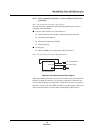
P295
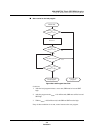
Figure 13-3 shows the MN102H75K
operation sequence in each of
these modes. In all modes, the I
2
C bus controller generates an interrupt
after each data byte transfer, then the software loads the next data byte
P295 Figure 13-3 shows the MN102H75K/85K
operation sequence in each
of these modes. In all modes, the I
2
C bus controller generates an inter-
rupt after each data byte transfer, then the software loads the next data
byte
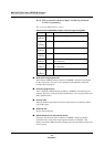
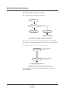
P299
Figure 13-6 and table 13-5 provide the timing definitions and specifica-
tions for the for the MN102H75K
I
2
C bus interface
P299 Figure 13-6 and table 13-5 provide the timing definitions and specifica-
tions for the for the MN102H75K/85K
I
2
C bus interface
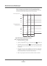
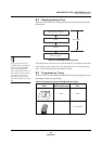
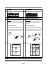
P301 Note: The circled areas are signals output from the MN102H75K
P301
Note: The circled areas are signals output from the MN102H75K/85K
P303
Note: The circled areas are signals output from the MN102H75K
P303
Note: The circled areas are signals output from the MN102H75K/85K