


Serial Interfaces
Serial Interface Setup Examples
Panasonic Semiconductor Development Company MN102H75K/F75K/85K/F85K LSI User Manual
136
Panasonic
Do not change the clock source
once you select it. Selecting the
clock source while you set up
the count operation control will
corrupt the value in the binary
counter.
3. Set the TM1LD bit of the TM1MD register to 1. This loads the value in the
base register to the binary counter. At the same time, select the clock source
as B
OSC
/4 by writing b’00’ to TM1S[1:0].
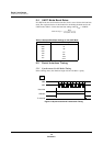
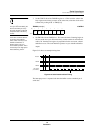
TM1MD (example) x’00FE21’
In the bank and linear address-
ing versions of the MN102
series, it was necessary to set
TM1EN and TM1LD to 0
between steps 3 and 4, to
ensure stable operation. This is
unnecessary in the high-speed
linear addressing version.
4. Set TM1LD to 0 and TM1EN to 1. This starts the timer. Counting begins at
the start of the next cycle. When the binary counter reaches 0 and loads the
value x’26’ from the base register, in preparation for the next count, a timer 1
underflow occurs. The serial interface operates in sync with this underflow
output.
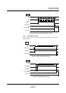
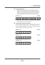
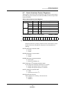
Figure 5-12 shows an example timing chart.
The interrupt process is repeated each time the buffer receives another byte of
serial data.
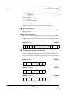
Bit:76543210
TM1
EN
TM1
LD
————
TM1
S1
TM1
S0
Setting:01000000
Figure 5-12 Serial Interface Clock Timing
26
B
OSC
/4
00
00 26 00 26 00 26 00 26 00 26 00 26 00 26 00 26 00 26 00 26 00 26
indicates 25, 24-02, and 01.
TM1BR
TM1BC
TM1 output
(To serial I/F)