


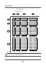
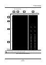

On-Screen Display
DMA and Interrupt Timing
MN102H75K/F75K/85K/F85K LSI User Manual Panasonic Semiconductor Development Company
191
Panasonic
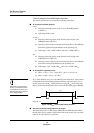
7.11 DMA and Interrupt Timing
This section describes how the MN102H75K/85K handles the timing of direct
memory access (DMA) transfers of OSD data and OSD interrupts.
■
DMA
If you use the OSD function, the
DMA function executes for both
the text and graphics layers,
even if your program does not
use one of these layers. To
prevent error, program data for
the unused layer to meet the
restrictions outlined in section
7.1, “Description,” on page 153.
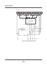
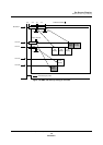
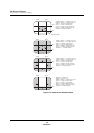
On both the text and graphics layers, the microcontroller reads the line 1 data
from the RAM as it scans line 1 onto the display. For line 2 and following lines, it
reads the data as it scans the display start for the preceding line. The RAM read
starts 12 system clock cycles (12T
S
) after the leading edge of the HSYNC pulse.
The DMA transfer takes 4T
S
for each display data word.
In line 1, or when a graphics and text line begin simultaneously, the data transfer
requests for both layers occur simultaneously. The text data transfer always takes
priority. The graphics data transfer begins 5T
S
after the text data transfer ends.
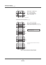
If a DMA transfer occurs at the same time as the leading edge of a VSYNC pulse,
the screen flickers. To avoid this, do not set a display position in the last line.
Interrupts
For both graphics and text displays, the microcontroller processes the GINT and
CINT interrupt request bits of the display data’s GVP and CVP fields during
DMA transfer. If GINT or CINT is set to 1, when the associated transfer ends
(GVP or CVP transfer) the OSD generates an interrupt request.
Note that if the interrupt bit is set to 1 in the line 1 display data, the interrupt
occurs at the first scan line. If the interrupt bit is set to 1 in the line 2 display data,
the interrupt occurs at the first display line.
■