


I
2
C Bus Controller
Setting Up the I
2
C Bus Connection
Panasonic Semiconductor Development Company MN102H75K/F75K/85K/F85K LSI User Manual
298
Panasonic
13.4 Setting Up the I
2
C Bus Connection
Set the I
2
C connection in the I2CSEL0 and I2CSEL1 bits of the PCNT0 register
(x’00FF90’). Since the SCL0, SDA0, SCL1, and SDA1 pins also serve as
general-purpose port pins, and reset to the general-purpose function, you must set
these bits every time the program uses the I
2
C function. You must also select the
I
2
C function in the port mode registers. For I
2
C bus connection 0, set bits 0 and 1
of the P6MD register (x’00FFFC’). For I
2
C bus connection 1, set bits 1 and 2 of
the P0MD register (x’00FFF0’).
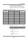
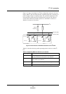
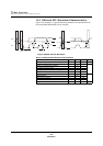
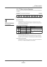
Table 13-4 shows the register settings required to use either SDA0/SCL0 or
SDA1/SCL1 alone, and figure 13-5 shows the control circuit for this pin setup.
Table 13-4 Registers Settings for SDA0/SCL0 or SDA1/SCL1 Ports
Register Bit SDA0, SCL0 Only SDA1, SCL1 Only
P0MD (x’00FFF0) 1 0 (selects P01) 1 (selects SDA1)
2 0 (selects P02) 1 (selects SCL1)
P6MD (x’00FFFC’) 0 1 (selects SDA0) 0 (selects P60)
1 1 (selects SCL0) 0 (selects P61)
PCNT0 (x’00FF90’) 8 1 (enables SDA0, SCL0) 0 (disables SDA0, SCL0)
9 0 (disables SDA1, SCL1) 1 (enables SDA1, SCL1)
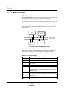
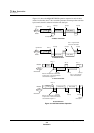
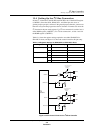
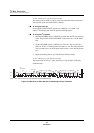
Figure 13-5 Pin Control Circuit for the I
2
C Bus Controller
I
2
C
Circuit
SDA IN
SCL OUT
SCL IN
SDA OUT
SDA
0
SDA1
SCL1
SCL0
I2CSEL0
Port control register 0
x'00FF90' bit 8
I2CSEL0
Port control register 0
x'00FF90' bit 8
I2CSEL0
x'00FF90' bit 9
I2CSEL0
x'00FF90' bit 9
1: on
0: off