


MN102H75K/F75K/85K/F85K LSI User Manual Panasonic Semiconductor Development Company
3
Panasonic
P33
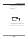
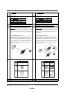
The MN102H75K contains an internal PLL circuit. To use this circuit,
you must connect it to an external (lag-lead) filter.
P34
The MN102H75K/85K contains an internal PLL circuit. To use this
circuit, you must connect it to an external (lag-lead) filter.
P37
The most important factor in real-time control is an MCU’s speed in
servicing interrupts. The MN102H75K
has an extremely fast interrupt
response time due to its ability to abort instructions, such as multiply or
divide, that require multiple clock cycles. The MN102H75K
re-
executes an aborted instruction after returning from the interrupt service
routine.
This section describes the interrupt system in the MN102H75K
. The
MN102H75K contains 36 interrupt group controllers. Each controls a
single interrupt group. Because each group contains only one interrupt
vector, the MN102H75K
can handle interrupts much quicker than pre-
viously possible. Each interrupt group belongs to one of twelve classes,
which defines its interrupt priority level.
With the exception of reset interrupts, all interrupts from timers, other
peripheral circuits, and external pins must be registered in an interrupt
group controller. Once they are registered, interrupt requests are sent to
the CPU in accordance with the interrupt mask level (0 to 6) set in the
interrupt group controller. Groups 1 to 3 are dedicated to system inter-
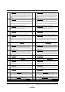
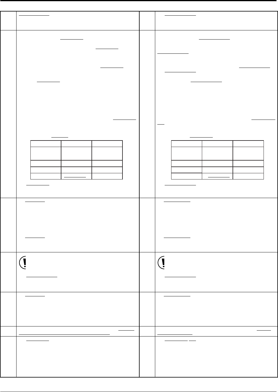
rupts. Table 2-1 compares the interrupt parameters of the MN102H75K
to those of the MN102L35G, the comparable MCU in the previous gen-
eration of the 16-bit series
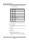
Table2-1Comparison of MN102H75K and MN102L35G Interrupt Features
The MN102H75K has six external interrupt pins. Set the interrupt con-
dition (positive edge, negative edge, either edge, or active low) in the
EXTMD register
P37
The most important factor in real-time control is an MCU’s speed in
servicing interrupts. The MN102H75K/85K
has an extremely fast
interrupt response time due to its ability to abort instructions, such as
multiply or divide, that require multiple clock cycles. The
MN102H75K/85K
re-executes an aborted instruction after returning
from the interrupt service routine.
This section describes the interrupt system in the MN102H75K/85K
.
The MN102H75K/85K
contains 36 interrupt group controllers. Each
controls a single interrupt group. Because each group contains only one
interrupt vector, the MN102H75K/85K
can handle interrupts much
quicker than previously possible. Each interrupt group belongs to one
of twelve classes, which defines its interrupt priority level.
With the exception of reset interrupts, all interrupts from timers, other
peripheral circuits, and external pins must be registered in an interrupt
group controller. Once they are registered, interrupt requests are sent to
the CPU in accordance with the interrupt mask level (0 to 6) set in the
interrupt group controller. Groups 1 to 3 are dedicated to system inter-
rupts. Table 2-1 compares the interrupt parameters of the MN102H75K/
85K to those of the MN102L35G, the comparable MCU in the previous
generation of the 16-bit series
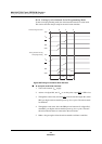
Table2-1Comparison of MN102H75K/85K and MN102L35G Interrupt Features
The MN102H75K/85K has six external interrupt pins. Set the interrupt
condition (positive edge, negative edge, either edge, or active low) in
the EXTMD register
P72
The MN102H75K provides two ways to reduce power consumption, controlling
CPU operating and standby modes to cut overall consumption and shutting down
unused functions by stopping the system clock supplied to them.
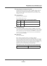
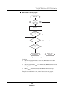
3.1 CPU Modes
3.1.1 Description
The MN102H75K has two CPU operating modes, NORMAL and SLOW, and two
CPU standby modes, HALT and STOP. Effective use of these modes can signifi-
cantly reduce power consumption. Figure 3-1 shows the CPU states in the different
modes
P72
The MN102H75K/85K provides two ways to reduce power consumption, con-
trolling CPU operating and standby modes to cut overall consumption and shutting
down unused functions by stopping the system clock supplied to them.
3.1 CPU Modes
3.1.1 Description
The MN102H75K/85K has two CPU operating modes, NORMAL and SLOW, and
two CPU standby modes, HALT and STOP. Effective use of these modes can sig-
nificantly reduce power consumption. Figure 3-1 shows the CPU states in the dif-
ferent modes
P73
The MN102H75K/85K
recovers from power up and reset in SLOW
mode. For normal operation, the program must switch the MCU from
SLOW to NORMAL mode
P73
The MN102H75K/85K
recovers from power up and reset in SLOW
mode. For normal operation, the program must switch the MCU from
SLOW to NORMAL mode
P73
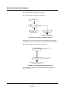
The MN102H75K contains a PLL circuit that, in NORMAL mode, multiplies the
clock input through the OSC1 and OSC2 pins by 12, divides the signal by 2, then
sends the resulting clock to the CPU. (See figure 3-2.) The MCU starts in SLOW
mode on power up and on recovery from a reset. In SLOW mode (system clock = 2
MHz), the clock from the OSC pins feeds directly to the CPU, without going
through the PLL circuit. This means that the program must switch the CPU from
SLOW to NORMAL mode (system clock = 12 MHz)
P73
The MN102H75K/85K contains a PLL circuit that, in NORMAL mode, multiplies
the clock input through the OSC1 and OSC2 pins by 12, divides the signal by 2,
then sends the resulting clock to the CPU. (See figure 3-2.) The MCU starts in
SLOW mode on power up and on recovery from a reset. In SLOW mode (system
clock = 2 MHz), the clock from the OSC pins feeds directly to the CPU, without
going through the PLL circuit. This means that the program must switch the CPU
from SLOW to NORMAL mode (system clock = 12 MHz)
P73
For information on invoking SLOW mode from NORMAL mode, see MN10200
Series Linear Addressing High-Speed Version LSI User Manual.
P73
For information on invoking SLOW mode from NORMAL mode, see MN102H
Series LSI User Manual.
P75
The MN102H75K
allows you to turn each peripheral function on or off
through writing to the registers. You can significantly reduce power
consumption by turning off unused functions. Table 3-1 shows the
register bits controlling on and off for each function block. The ADC
used for the OSD and CCD functions is turned off on reset. Write a 1 to
the function to enable it, when necessary
P75
The MN102H75K/85K allows you to turn each peripheral function on
or off through writing to the registers. You can significantly reduce
power consumption by turning off unused functions. Table 3-1 shows
the register bits controlling on and off for each function block. The
ADC used for the OSD and CCD functions is turned off on reset. Write
a 1 to the function to enable it, when necessary
Parameter
MN102L35G
MN102H75K
interrupt groups
(IAGR group numbers)
4 vectors per group
(Separated by interrupt
service routine)
1 vector per group
(Group number gener-
ated for each interrupt)
interrupt response time
interrupt level settings
Software compatibility
Good
4 vectors per level
Excellent
4 vectors per level
Easily modified
Parameter
MN102L35G
MN102H75K/85K
interrupt groups
(IAGR group numbers)
4 vectors per group
(Separated by interrupt
service routine)
1 vector per group
(Group number gener-
ated for each interrupt)
interrupt response time
interrupt level settings
Software compatibility
Good
4 vectors per level
Excellent
4 vectors per level
Easily modified