


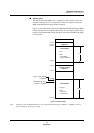
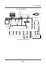
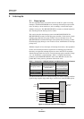

General Description
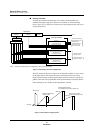
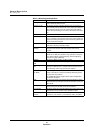
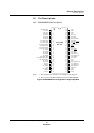
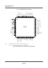
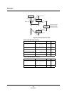
Pin Descriptions
Panasonic Semiconductor Development Company MN102H75K/F75K/85K/F85K LSI User Manual
32
Panasonic
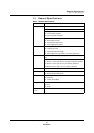
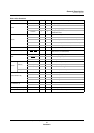
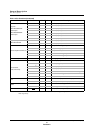
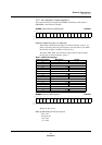
Table 1-3 Pin Functions
Block Pin Name I/O Pin Count Description
Power
V
DD
I 1 Voltage supply
V
SS
I 2 Ground reference
AV
DD
I 1 Analog voltage supply
V
DD
/V
PP
I1
Voltage supply: V
DD
in mask ROM version and V
PP
in
EEPROM version
Clocks
SYSCLK O 1 System clock output
OSC1 I 1 Oscillator input connection (with internal PLL)
OSC2 O 1 Oscillator output connection (with internal PLL)
OSDXI I 1 OSD oscillator input connection (alt. function: P46)
OSDXO O 1 OSD oscillator output connection (alt. function: P45)
Reset RST
I/O 1 Reset
(alt. function: P53)
Interrupts (external) IRQ0–IRQ5 I6
External interrupt request to microcontroller (alt. functions:
P00, P10, P11, P12, P52, P54)
OSD
HSYNC
I 1 Horizontal sync signal input
VSYNC
I 1 Vertical sync signal input
YS O 1 Video signal cut
Timers
16-bit (2)
TMnIOA (n=4,5) I/O 2 Input capture/output compare A
TMnIOB (n=4,5) I/O 2 Input capture/output compare B
TMnIC (n=4,5) I 2 Timer/counter clear signal
8-bit (4) TMnIO (n=0,1) I/O 2 Timer clock input/timer output
Serial interfaces (2)
SBI0/SBI1 I 2 Serial data input
SBD0/SBD1 I/O 2 Serial data input
SBO0/SBO1 I/O 2 Serial data output
SBT0/SBT1 I/O 2 Serial clock signal
I
2
C interfaces (2)
SDA0/SDA1 I/O 2 I
2
C data
SCL0/SCL1 I/O 2 I
2
C clock
IR remote signal receiver RMIN I 1 Remote signal input
PWM (8-bit, 7-channel) PWM0–PWM6 O 7 Pulse width modulator output