


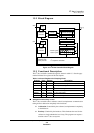
I
2
C Bus Controller
I
2
C Bus Interface Registers
Panasonic Semiconductor Development Company MN102H75K/F75K/85K/F85K LSI User Manual
304
Panasonic
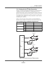
13.7 I
2
C Bus Interface Registers
All registers in I
2
C blook cannot be written by byte (by word only). Read by byte
is possible.
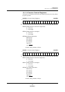
I2CDTRM: I
2
C Transmission Data Register x’007E40’
SCL is held low during interrupt
servicing, and is cleared high by
a write to I2CDTRM.
STA: I
2
C start control
STO: I
2
C stop control
Writing to the STA and STO bits allows you to change the state of the
transmission or reception operation. Table 13-6 shows the settings for dif-
ferent start and stop conditions.
ACK: Acknowledge signal output control
The acknowledge signal is output after every byte transfer, on the ninth
clock pulse. ACK is normally 1 and transitions to 0 to output an acknowl-
edge (for instance if the master or slave receiver has received a data byte).
DT[7:0]: Data to be transmitted
The parallel data in this field is converted to serial data for transmission to
the I
2
C bus. It is shifted out MSB first to the interface.
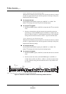
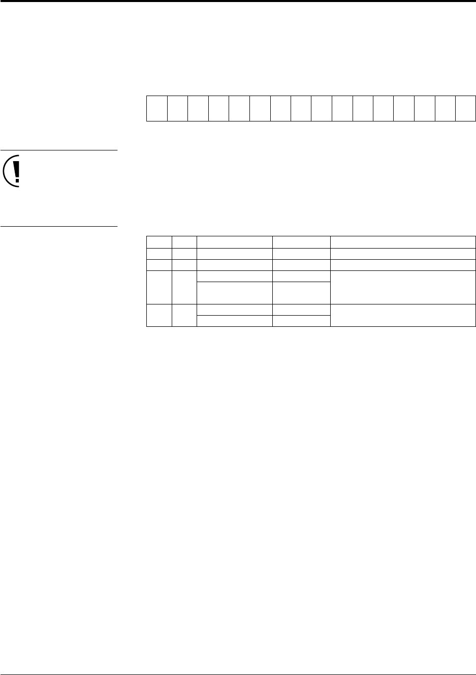
Bit:1514131211109876543210
—————STASTOACKDT7DT6DT5DT4DT3DT2DT1DT0
Reset:0000000000000000
R/W:RRRRRR/WR/WR/WR/WR/WR/WR/WR/WR/WR/WR/W
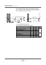
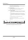
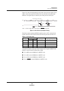
Table 13-6 STA and STO Settings
STA STO Mode Function Description
00All NOP No state change
11All NOP No state change
10Slave receiver Start Change to mode indicated by R/W bit.
R/W = 0: Change to master transmitter
R/W = 1: Change to master receiver
Master transmitter Repeat start
01Slave receiver Stop read Change to slave receiver after stop
condition.Master transmitter Stop write