


Closed-Caption Decoder
Closed-Caption Decoder Registers
MN102H75K/F75K/85K/F85K LSI User Manual Panasonic Semiconductor Development Company
243
Panasonic
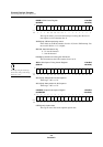
FQSEL: Frequency Select Register x’007EC2’
(FQSELW x’007EE2’)
In this register, set the sampling cycle for separating the HSYNC and
VSYNC signals from the composite sync signal. The recommended setting
is x’1F01’.
VFQDIV[5:0]: Sampling frequency setting for VSYNC separator
In this field, set the ratio by which to divide the sampling frequency for the
HSYNC separator.
FQDIV[3:0]: Sampling frequency setting for HSYNC separator
In this field, set the ratio by which to divide the A/D sampling frequency.
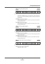
SCMING: Minimum Sync Level Detection Interval Set Register x’007EC4’
(SCMINGW x’007EE4’)
SCMING[9:0]: Interval setting for the minimum sync level detection
Set the HSYNC cycle in this field in ADC clock units. This is the interval
used for detecting the sync tip level for sync tip clamping. The valid range
is x’000’ to x’3FF’. Note that the HSYNC cycle set in this register is only
used for detecting the minimum sync level. You must also set the correc-
tion HSYNC cycle in HSEP1.
For the NTSC format, the setting for this register is x’02FA’, calculated as
follows:
(A/D sampling frequency) × (HSYNC cycle) = 12 MHz × 63 µs = x’02FA’
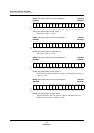
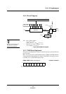
BPPST: Backporch Position Register x’007EC6’
(BPPSTW x’007EE6’)
BPPST[8:0]: Backporch start position for the leading edge of HSYNC
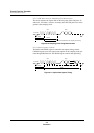
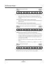
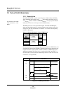
Bit:1514131211109876543210
——
VFQ
DIV5
VFQ
DIV4
VFQ
DIV3
VFQ
DIV2
VFQ
DIV1
VFQ
DIV0
————
FQ
DIV3
FQ
DIV2
FQ
DIV1
FQ
DIV0
Reset:0011111100000001
R/W: R R R/W R/W R/W R/W R/W R/W R R R R R/W R/W R/W R/W
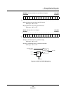
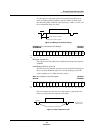
Bit:1514131211109876543210
——————
SC
MING
9
SC
MING
8
SC
MING
7
SC
MING
6
SC
MING
5
SC
MING
4
SC
MING
3
SC
MING
2
SC
MING
1
SC
MING
0
Reset:0000001100000000
R/W:RRRRRRR/WR/WR/WR/WR/WR/WR/WR/WR/WR/W
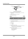
Bit:1514131211109876543210
———————
BP
PST8
BP
PST7
BP
PST6
BP
PST5
BP
PST4
BP
PST3
BP
PST2
BP
PST1
BP
PST0
Reset:0000000000111100
R/W:RRRRRRRR/WR/WR/WR/WR/WR/WR/WR/WR/W