


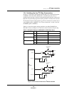

I
2
C Bus Controller
I
2
C Bus Interface Registers
Panasonic Semiconductor Development Company MN102H75K/F75K/85K/F85K LSI User Manual
306
Panasonic
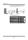
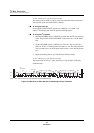
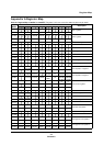
I2CCLK: I
2
C Clock Control Register x’007E46’
To conform to the specification,
the clock signal must be
between 0 and 100 kHz. To sat-
isfy this requirement, always set
I2CCLK to x’032’ or higher.
C[9:0]: Output clock frequency select
This 10-bit field determines the SCL output. With a 12-MHz system clock,
calculate the frequency as follows:
In this case, the following settings apply:
x’032’: 100 kHz x’06E’: 50 kHz
x’039’: 89.6 kHz x’08C’: 40 kHz
x’041’: 80 kHz x’0BE’:30 kHz
x’04C’: 69.8 kHz x’122’: 20 kHz
x’05A’: 60 kHz x’24E’: 10 kHz
I2CBRST: I
2
C Bus Reset Register x’007E48’
BRST: Bus reset
When a serious bus error occurs, this bit can be set to 0, forcing the clock
line low and resetting the I
2
C bus. This function works in all I
2
C modes.
After a forced reset, the microcontroller is in slave receiver mode. This reset
does not change the contents of the I2CMYAD and I2CCLK registers.
0: Force bus to reset
1: Steady state
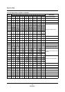
I2CBSTS: I
2
C Bus Status Register x’007E4A’
I2CBSTS is a two-bit, read-only register that monitors the status of the I
2
C
bus.
SDAS: SDA data line status
This bit monitors the state of the I
2
C data line, SDA.
SCLS: SCL clock line status
This bit monitors the state of the I
2
C clock line, SCL.
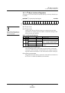
Bit:1514131211109876543210
——————C9C8C7C6C5C4C3C2C1C0
Reset:0000000000000000
R/W:RRRRRRR/WR/WR/WR/WR/WR/WR/WR/WR/WR/W
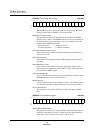
Bit:1514131211109876543210
———————————————BRST
Reset:0000000000000001
R/W:RRRRRRRRRRRRRRRR/W
Bit:1514131211109876543210
——————————————SDASSCLS
Reset:0000000000000000
R/W:RRRRRRRRRRRRRRRR
f
SCL
12 MHz
2 Register setting 10+()×
---------------------------------------------------------------------=