


ROM Correction
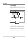
Block Diagram
MN102H75K/F75K/85K/F85K LSI User Manual Panasonic Semiconductor Development Company
289
Panasonic
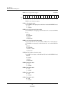
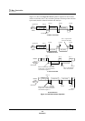
12.2 Block Diagram
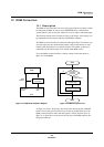
Figure 12-3 is a block diagram of the ROM correction circuit. A match detection
circuit constantly monitors the ROM address specified by the CPU instruction
pointer (IP). When the value matches a correction address, the circuit replaces the
data output from the ROM with the data in the appropriate correction data
register. It then sends the corrected data to the CPU.
12.3 Programming Considerations
At reset, the ROM correction address match and data registers contain all 0s.
Since a reset also disables ROM correction (in ROMCEN), the ROM will still
operate normally.
Only read from or write to the address match registers while ROM correction is
disabled in ROMCEN. Otherwise, an error may occur in the match detection circuit.
Note that the address match and data registers only allow full-register access (8-
bit or 16-bit depending on the register). You cannot write to individual bits.
Figure 12-3 ROM Correction Block Diagram
Data bus
ROM
address
CPU
IP
MUX (selector)
ROM correction
enable
registers
Match
detection
circuit
ROM
Correction
data
registers
Correction
address
match
registers
Correction
address
Correction
data