


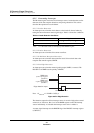
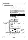

Closed-Caption Decoder
Functional Description
MN102H75K/F75K/85K/F85K LSI User Manual Panasonic Semiconductor Development Company
229
Panasonic
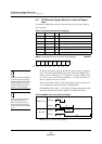
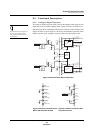
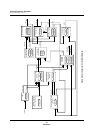
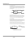
9.3.2 Clamping Circuit
This block clamps the input video signal (CVBS0, CVBS1).
The clamping circuit internal to the MN102H75K/85K provides three current
sources—high, medium, and low. You can modify these current sources using
external resistors R1 and R2. Within the clamping circuit, you can turn each of the
current sources on and off in steps. The control bits for these currents are the same
for sync tip and pedestal clamping, but the reference and compare levels are dif-
ferent. Table 9-3 provides these values for the two types of clamping, and table 9-4
shows how to control the three current levels so that the video signal matches the
reference level.
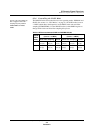
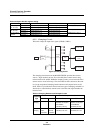
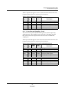
Table 9-2 Caption decoder register setting
VBI control ADC control Clamp control
Use two cap-
tion decoders
caption 0 ON(PCNT0.bp0=0) ON(PCNT0.bp4=1) (P3MD.bp3,2,1)=(0,1,1)
caption 1 ON(PCNT0.bp1=0) ON(PCNT0.bp5=1)
Use one cap-
tion decoder
caption 0 ON(PCNT0.bp0=0) ON(PCNT0.bp4=1) (P3MD.bp3,2,1)=(1,0,1)
no caption 1 OFF(PCNT0.bp1=1) OFF(PCNT0.bp5=0)
No use caption
decoder
no caption 0 OFF(PCNT0.bp0=1) OFF(PCNT0.bp4=0) (P3MD.bp3,2,1)=(0,0,0)
no caption 1 OFF(PCNT0.bp1=1) OFF(PCNT0.bp5=0)
Figure 9-5 Clamping Circuit
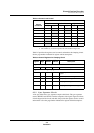
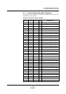
Table 9-3 Clamping Reference and Compare Levels
Clamping
Type
Reference Level Compare Level
CCD0 CCD1 CCD0 CCD1
Sync tip
clamping
16 (dec) 16 (dec) Output from minimum
detection circuit (value
in SYNCMIN,
x’007EC8’, bits 6-0)
Output from minimum
detection circuit (value
in SYNCMINW,
x’007EE8’, bits 6-0)
Pedestal
clamping
Value in
PCLV,
x’007ECC’
Value in
PCLVW,
x’007EEC’
Value in SYNCMIN,
x’007EC8’, bits 14-8
Value in SYNCMINW,
x’007EE8’, bits 14-8
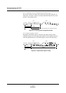
A/D
ADDATA[7:0]
CVBS0, 1
CLL
CLH
3.3 V
1
3
5
2
4
6
Control circuit
Data slice
circuit
External
circuit
Sync separator
Clamping
Circuit
6.8 kΩ
33 kΩ
Vidio in