


Closed-Caption Decoder
Closed-Caption Decoder Registers
Panasonic Semiconductor Development Company MN102H75K/F75K/85K/F85K LSI User Manual
240
Panasonic
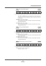
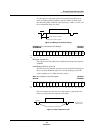
CRIFA: CRI Frequency Width Register A x’007E0C’
(CRIFAW x’007E2C’)
The CRIFA and CRIFB registers store the CRI cycles from rising edge to
rising edge, for monitoring whether the CRIs were detected correctly dur-
ing this period.
CRI2FQW[7:0]: CRI frequency width 2
This field indicates the width, in clock units, from the second to the third
rising edge after the CRI.
CRI1FQW[7:0]: CRI frequency width 1
This field indicates the width, in clock units, from the first to the second
rising edge after the CRI.
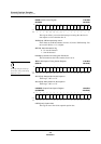
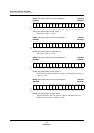
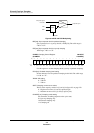
CRIFB: CRI Frequency Width Register B x’007E0E’
(CRIFBW x’007E2E’)
CRI4FQW[7:0]: CRI frequency width 4
This field indicates the width, in clock units, from the fourth to the fifth ris-
ing edge after the CRI.
CRI3FQW[7:0]: CRI frequency width 3
This field indicates the width, in clock units, from the third to the fourth
rising edge after the CRI.
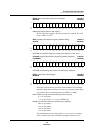
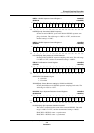
CRI1S: CRI Capture Start Timing Control Register 1 x’007E10’
(CRI1SW x’007E30’)
CRI1S[10:0]: Start position for CRI capture 1
Valid range: x’000’ to x’7FF’
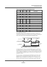
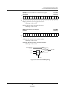
Bit:1514131211109876543210
CRI2
FQW7
CRI2
FQW6
CRI2
FQW5
CRI2
FQW4
CRI2
FQW3
CRI2
FQW2
CRI2
FQW1
CRI2
FQW0
CRI1
FQW7
CRI1
FQW6
CRI1
FQW5
CRI1
FQW4
CRI1
FQW3
CRI1
FQW2
CRI1
FQW1
CRI1
FQW0
Reset:0000000000000000
R/W:RRRRRRRRRRRRRRRR
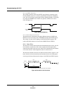
Bit:1514131211109876543210
CRI4
FQW7
CRI4
FQW6
CRI4
FQW5
CRI4
FQW4
CRI4
FQW3
CRI4
FQW2
CRI4
FQW1
CRI4
FQW0
CRI3
FQW7
CRI3
FQW6
CRI3
FQW5
CRI3
FQW4
CRI3
FQW3
CRI3
FQW2
CRI3
FQW1
CRI3
FQW0
Reset:0000000000000000
R/W:RRRRRRRRRRRRRRRR
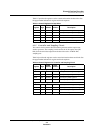
Bit:1514131211109876543210
—————
CRI1S
10
CRI1S
9
CRI1S
8
CRI1S
7
CRI1S
6
CRI1S
5
CRI1S
4
CRI1S
3
CRI1S
2
CRI1S
1
CRI1S
0
Reset:0000011111111111
R/W:RRRRRR/WR/WR/WR/WR/WR/WR/WR/WR/WR/WR/W