


Timers
16-Bit Timer Control Registers
MN102H75K/F75K/85K/F85K LSI User Manual Panasonic Semiconductor Development Company
125
Panasonic
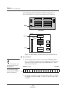
4.12 16-Bit Timer Control Registers
Table 4-6 shows the registers used to control the 16-bit timers. A binary counter
(TMnBC), a compare/capture register A (TMnCA), a compare/capture register B
(TMnCB), and a timer mode register (TMnMD) is associated with each 16-bit
timer.
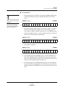
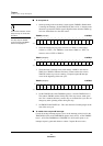
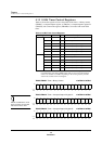
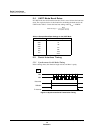
TM4BC/TM5BC: Timer n Binary Counter x’00FE82’/x’00FE92’
TMnCA and TMnCB are 16-bit
access registers. Use the MOV
instruction to write to them.
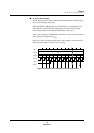
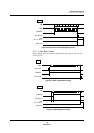
TM4CA/TM5CA: Timer n Compare/Capture Register A x’00FE84’/x’00FE94’
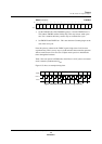
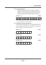
TM4CB/TM5CB: Timer n Compare/Capture Register B x’00FE88’/x’00FE98’
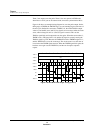
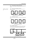
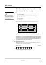
Table 4-6 16-Bit Timer Control Registers
Register Address R/W Description
Timer 4 TM4MD x’00FE80’ R/W Timer 4 mode register
TM4BC x’00FE82’ R Timer 4 binary counter
TM4CA x’00FE84’ R/W Timer 4 compare/capture register A
TM4CAX x’00FE86’ — Timer 4 compare/capture register set AX
TM4CB x’00FE88’ R/W Timer 4 compare/capture register B
TM4CBX x’00FE8A’ — Timer 4 compare/capture register set BX
Timer 5 TM5MD x’00FE90’ R/W Timer 5 mode register
TM5BC x’00FE92’ R Timer 5 binary counter
TM5CA x’00FE94’ R/W Timer 5 compare/capture register A
TM5CAX x’00FE96’ — Timer 5 compare/capture register set AX
TM5CB x’00FE98’ R/W Timer 5 compare/capture register B
TM5CBX x’00FE9A’ — Timer 5 compare/capture register set BX
Note: TM4CAX, TM4CBX, TM5CAX, and TM5CBX are virtual registers used only
in double-buffer mode during PWM output. They do not exist in the hardware
and are not readable or writable. Depending on the write signal, they load the
value in the associated CA or CB register.
Bit:1514131211109876543210
TMn
BC15
TMn
BC14
TMn
BC13
TMn
BC12
TMn
BC11
TMn
BC10
TMn
BC9
TMn
BC8
TMn
BC7
TMn
BC6
TMn
BC5
TMn
BC4
TMn
BC3
TMn
BC2
TMn
BC1
TMn
BC0
Reset:0000000000000000
R/W:RRRRRRRRRRRRRRRR
Bit:1514131211109876543210
TMn
CA15
TMn
CA14
TMn
CA13
TMn
CA12
TMn
CA11
TMn
CA10
TMn
CA9
TMn
CA8
TMn
CA7
TMn
CA6
TMn
CA5
TMn
CA4
TMn
CA3
TMn
CA2
TMn
CA1
TMn
CA0
Reset:0000000000000000
R/W: R/W R/W R/W R/W R/W R/W R/W R/W R/W R/W R/W R/W R/W R/W R/W R/W
Bit:1514131211109876543210
TMn
CB15
TMn
CB14
TMn
CB13
TMn
CB12
TMn
CB11
TMn
CB10
TMn
CB9
TMn
CB8
TMn
CB7
TMn
CB6
TMn
CB5
TMn
CB4
TMn
CB3
TMn
CB2
TMn
CB1
TMn
CB0
Reset:0000000000000000
R/W: R/W R/W R/W R/W R/W R/W R/W R/W R/W R/W R/W R/W R/W R/W R/W R/W