


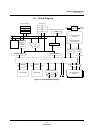

General Description
Bus Interface
Panasonic Semiconductor Development Company MN102H75K/F75K/85K/F85K LSI User Manual
36
Panasonic
1.7.2 Bus Interface Control Registers
The external memory wait register (EXWMD) and memory mode register 1
(MEMMD1) control the bus interface.
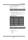
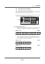
EXWMD: External Memory Wait Register x’00FF80’
EW[33:30], EW[23:20], EW[13:10], EW[03:00]
These fields contain the wait settings for external memory spaces 3, 2, 1,
and 0, respectively. One wait corresponds to one instruction cycle. When
the external oscillator is 4 MHz, one wait is 83 ns.
The OSD, VBI0, VBI1, I2C, IR remote signal receiver, and H counter
blocks apply to external memory space 0.
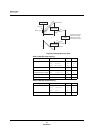
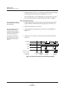
MEMMD1: Memory Mode Register 1 x’00FF82’
Write 0s to bits 15 to 2.
IOW[1:0]: Wait setting for internal I/O space
00: 1 wait
01: Reserved
10: 2 waits
11: 3 waits
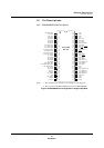
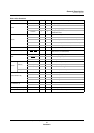
Bit:1514131211109876543210
EW 33 EW 32 EW 31 EW 30 EW 23 EW 22 EW 21 EW 20 EW 13 EW 12 EW 11 EW 10 EW 03 EW 02 EW 01 EW 00
Reset:1110111011101110
R/W: R/WR/WR/WR/WR/WR/WR/WR/WR/WR/WR/WR/WR/WR/WR/WR/W
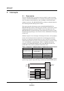
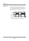
Table 1-4 Wait Count Settings
EW[n3:n0] Setting Wait Count Cycles
0000 0.01.0
0001 R eserved
0010 1.02.0
0011 R eserved
0100 2.03.0
0101 R eserved
0110 3.04.0
0111 Reserved
1000 4.05.0
1001 R eserved
1010 5.06.0
1011 R eserved
1100 6.07.0
1101 R eserved
1110 7.08.0
1111 R eserved
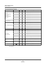
Bit:1514131211109876543210
EB31 EB32 EB21 EB20 EB11 EB10 EB01 EB00 BRS1 BRS0 BRC3 BRC2 BRC1 BRC0 IOW1 IOW0
Reset:0000000000000011
R/W: R/WR/WR/WR/WR/WR/WR/WR/WR/WR/WR/WR/WR/WR/WR/WR/W