


I
2
C Bus Controller
Description
Panasonic Semiconductor Development Company MN102H75K/F75K/85K/F85K LSI User Manual
294
Panasonic
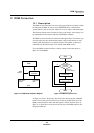
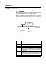
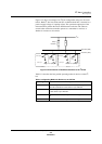
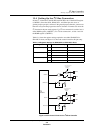
Figure 13-2 shows an example of an I
2
C bus configuration using two microcon-
trollers. Both I
2
C bus lines, SDA and SCL are bidirectional lines, connected to a
positive supply voltage via a pullup resistor. The open-drain output pins of the
microcontrollers perform the wired-AND function on the bus. The software
controls when each microcontroller operates as a transmitter or receiver, or
whether is in master or slave mode.
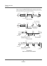
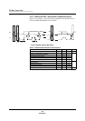
Table 13-2 describes the four possible operating modes for devices on the I
2
C
bus.
Figure 13-2 Connection of Two Microcontrollers to the I
2
C Bus
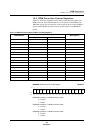
Table 13-2 Operating Modes for Devices on an I
2
C Bus
Operating Mode Description
Master transmitter Device that generates the serial transfer clock (SCL) signal and
transmits serial data to a slave device in sync with SCL
Master receiver Device that generates the SCL signal and receives serial data from
a slave device in sync with SCL
Slave transmitter Device that transmits data in sync with the SCL signal from the mas-
ter
Slave receiver Device that receives data in sync with the SCL signal from the master
Data line (SDA)
Clock line (SCL)
R
Pullup
resistors
V
DD
R
Clock output
Clock input
Data
output
Data input
Clock output
Clock input
Data
output
Data input
Device 1
Device 2