


Timers
16-Bit Timer Setup Examples
Panasonic Semiconductor Development Company MN102H75K/F75K/85K/F85K LSI User Manual
96
Panasonic
4.11.2 Setting Up a Single-Phase PWM Output Signal Using
Timer 4
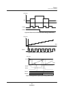
In this example, timer 4 is used to divide B
OSC
by 5 and generate a five-cycle,
single-phase PWM signal. The duty of this signal is 2:3. To accomplish this, the
program must load the divide-by ratio of 5 (actual setting: 4) into compare/
capture register A and a cycle count of 2 (actual setting: 1) into compare/capture
register B.
■
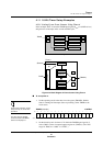
To set up the output port:
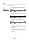
Set the P2MD[13:12] bits of the port 2 output mode register (P2MD) to b’01’
(selecting the TM4IOA pin) and set the P2DIR6 bit of the port 2 I/O control
register (P2DIR) to 1 (selecting output direction). This step selects the TM4OA
pin (P26) as the timer output port.
P2MD (example) x’00FFF4’
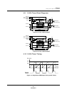
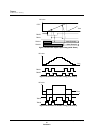
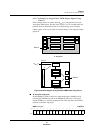
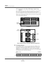
A. Chip Level
B. Block Level
Figure 4-29 Block Diagram of Single-Phase PWM Output Using Timer 4
TM4OA
P3
P6
PC
P4
P5
CORE
Interrupts
Timers 0-3
Timers 4-5
ROM, RAM
Bus Controller
Serial I/Fs
ADC
P2
B
OSC
/4
up
TM4BC
Timer 4
TM4CA
TM4CAX
TM4CB
TM4CBX
TM4OA
TQ
TQ
R
S
Q
Controller
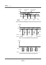
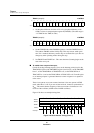
Bit:1514131211109876543210
—
P2
MD14
P2
MD13
P2
MD12
P2
MD11
P2
MD10
P2
MD9
P2
MD8
P2
MD7
P2
MD6
P2
MD5
P2
MD4
P2
MD3
P2
MD2
P2
MD1
P2
MD0
Setting:0001000000000000