


Analog-to-Digital Converter
Description
MN102H75K/F75K/85K/F85K LSI User Manual Panasonic Semiconductor Development Company
143
Panasonic
6 Analog-to-Digital Converter
6.1 Description
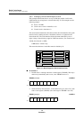
The MN102H75K/85K contains an 8-bit charge redistribution A/D converter
(ADC) that can process up to 12 channels. The reference clock is selectable to
B
OSC
x 1/8 or 1/16. When B
OSC
is 24 MHz, you must set the reference clock to
B
OSC
/8 (conversion rate = 4 µs) or higher.
6.2 Features
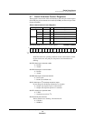
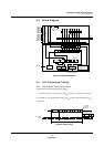
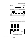
Figure 6-1 ADC Architecture
V
DD
ADIN0
ADIN1
ADIN2
ADIN3
ADIN4
ADIN5
ADIN6
ADIN7
ADIN8
ADIN9
ADIN10
ADIN11
V
SS
Sample
and
hold
8-bit
successive-
approximation
ADC
AN0BUF
AN1BUF
AN2BUF
AN3BUF
AN4BUF
AN5BUF
AN6BUF
AN7BUF
AN8BUF
AN9BUF
AN10BUF
AN11BUF
M
U
X
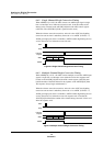
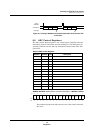
Table 6-1 ADC Functions and Features
Function/Feature Description
Sample and hold Embedded
Conversion time 4 µs per channel (when B
OSC
= 24 MHz)
Clock sources Programmable to B
OSC
divided by 8 or 16
Operating modes 46 operating modes (four types)
(1)
• Single conversion of one input (channel 0, 1, 2, 3, 4, 5, 6, 7, 8, 9, 10, or 11)
• Single conversion of multiple inputs (channels 0–n, where n = 1–11)
• Continuous conversion of one input (channel 0, 1, 2, 3, 4, 5, 6, 7, 8, 9, 10, or 11)
• Continuous conversion of multiple inputs (channels 0–n, where n = 1–11)
Conversion start Timer 1 underflow or register setting
Interrupts An interrupt is generated each time a single or continuous conversion sequence ends
Note: 1. Channels correspond to the ADIN pin having the same number. For instance, channel 3 (or ch3) corresponds to
ADIN3.