


Analog-to-Digital Converter
ADC Setup Examples
MN102H75K/F75K/85K/F85K LSI User Manual Panasonic Semiconductor Development Company
147
Panasonic
6.5 ADC Setup Examples
6.5.1 Setting Up Software-Controlled Single-Channel A/D Conversion
This example illustrates single-channel conversion controlled by the software.
The ADIN6 pin inputs an analog voltage signal (0.0 V–3.3 V) and the ADC
converts it to 8-bit digital values.
■
To set up the input port:
Set the P1MD2 bit of the port 1 output mode register (P1MD) to 1. This sets the
ADIN6 pin (P11) to analog input.
■
To set up the ADC:
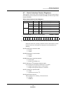
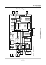
1. Set the operating conditions in the ADC control register (ANCTR). Select
single-channel, single-conversion mode (ANMD[1:0] = b’00’), B
OSC
/8 as
the clock source (ANCK[1:0] = b’10’), and channel 6 as the conversion
channel (AN1CH[3:0] = b’011’). Set the conversion start/busy bit, ANEN,
to 0.
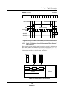
ANCTR (example) x’00FF00’
When the software controls the
conversion start, it must set the
ANEN flag to 1.
2. Set ANEN to 1 to start conversion. Conversion starts on the first rising edge
of the ADC clock after ANEN is set. The conversion time is 12 cycles of the
ADC clock. When B
OSC
= 24 MHz, this is 4.0 µs, or 4.0µs–4.3 µs after
ANEN is set.
The ADC can also generate an
interrupt when the conversion
ends, once the data is stored in
AN6BUF. In this case, the
software does not need to wait
for the ANEN flag before reading
AN6BUF.
3. Wait for the conversion to end. Since ANEN remains high during conver-
sion, then clears to 0, the program must wait until ANEN is 0.
4. Read the ADIN6 conversion data buffer (AN6BUF). The converter divides 0
to 3.3 volts into 256 segments, so the digital result is a value from 0 to 255.
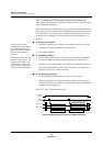
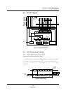
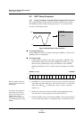
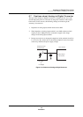
Figure 6-8 Single-Channel A/D Conversion
3.3 V
0 V
MN102H75K
P11, ADIN6
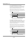
Bit:1514131211109876543210
AN
NCH3
AN
NCH2
AN
NCH1
AN
NCH0
AN
1CH3
AN
1CH2
AN
1CH1
AN
1CH0
AN
EN
AN
TC
——
AN
CK1
AN
CK0
AN
MD1
AN
MD0
Setting:0000011000001000