AGP Subsystem
7-4 Intel® 460GX Chipset Software Developer’s Manual
7.1.1.1 Page Sizes
The Itanium processor supports both a 4kB and a 4 MB page size. The AGP programming model is
designed using 4kB pages for GART entries. Using the larger page size would greatly reduce the
number of misses and reduce the number of entries needed in the GART, thus lowering system
cost.
The GXB will support 4 MB pages. Using 4 MB pages, 256kB of SRAM could provide 256 GB of
AGP space. The 460GX chipset will not support more than 32 GB of translatable graphics space.
7.1.1.2 GTLB
The GXB does not implement any GTLB or hold any old translations. Each address received by the
GXB will be translated through the SRAM.
7.1.1.3 Parity
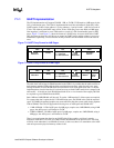
There is one parity bit which covers each GART entry. The parity covers the entire GART entry,
including reserved bits. The parity bit is generated by hardware. Software does not need to
compute parity for the GART entry. Software should mask out the parity bit and treat it as a
reserved bit on GART reads. The parity bit is returned on a read, so that it can be read by
diagnostics. Writing a zero or a one to the parity bit has no affect since the hardware will compute
correct parity and write that into the SRAM, which may cause the bit to be read as different from
what was written. Parity will be done such that the total number of 1’s, including the parity bit, total
to an even number.
7.1.2 Programming GART
The addresses to load or read the GART itself lie in the chipset specific area below 4 GB. There is
a 12 MB area for the chipset to use. The GART will exist in this range.
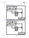
The GART lies at address range FE20_0000h to FE3F_FFFFh. GART entries may be read or
written from the processor. Accesses by the processor must be 4 byte accesses on an aligned 4B
boundary. Any other type of access is considered an error and the system will fault. For the Dual-
Expander bus GXB which attaches to Expander ports 2 and 3, it will be programmed through port
2 addresses only.
To the GXB, address bits 22 and 21 are don’t cares and shouldn’t be used in the decode for any
access at FEzx_xxxxh, where z is 0xx0 (binary). Address bit 23 must be a 0 for the address to point
to the GART. Address bit 20 must be a 0 also. The range FE30_0000h to FE3F_FFFFh is not
decoded by the GXB as a GART access, but is present in the address map for future growth.
When programming the GART, software must read the last location written, to guarantee that all
writes have taken affect. All writes to the GART table are done in order, so only the last write
address needs to be read. This ensures the GART table is updated in SRAM before allowing the
graphics cards to try and access translatable space. The processor must map the area from (4 GB-32
MB) to (4 GB-20 MB) as UC.


