WXB Hot-Plug
8-4 Intel® 460GX Chipset Software Developer’s Manual
8.1.4 PCICMD: PCI Command Register
Address Offset: 04h-05h Size: 16 bits
Default Value: 0000h Attribute: Partial Read/Write
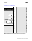
The PCI command register provides control over the IHPC’s ability to generate and respond to PCI
cycles. When a zero (0) is written to this register, the IHPC is logically disconnected from the PCI
bus for all accesses except configuration. The register bit list below shows the layout of the
register, explains the meanings of the different bits in the command register, gives the default value
of this register upon power-up, and gives the specific implementation of individual bits in the IHPC
(i.e. R/O or R/W).
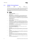
Bits
Description
15:10 reserved (0)
9 Fast Back-to-Back Enable
This bit is not supported. Hardwired Value = 0.
8 SERR# Enable
This bit is an enable bit for the SERR# driver. A value of zero (0) disables the SERR#
driver. A value of one (1) enables the SERR# driver. WXB configuration space
PCICMD(6) must be set to 1 to permit WXB SERR# pin assertion. Since the IHPC is
integrated into the WXB and is not addressable from the local PCI bus segment, the IHPC
will not report address parity errors via SERR#. This bit is configurable in the IHPC with
a default value of zero (0).
7 Wait Cycle Control
This bit is not supported. Hardwired Value = 0.
6 Parity Error Enable
This bit controls a device’s response to IHPC configuration and memory write parity
errors. When the bit is 1, the IHPC will assert both the Detected Parity Error status bit and
the PERR# output upon detection of an error. When the bit is 0, the IHPC will assert the
Detected Parity Error status on an error but will not assert PERR#. This bit must be set to
zero (0) after RST#. This bit is configurable in the IHPC with the default value zero (0).
5 VGA Palette Snoop
This bit controls how VGA-compatible devices handle accesses to their palette registers.
This bit is always set to zero (0) in the IHPC (disabled).
4 Memory Write and Invalidate Enable
This is an enable bit for using the memory write and invalidate command. This bit is
always set to zero (0) in the IHPC (disabled).
3 Special Cycle
This bit controls a device’s action on special cycle operations. A value of zero (0) causes
the device to ignore all special cycle operations. This bit is always set to zero (0) in the
IHPC.
2 Bus Master
This bit controls a device’s ability to act as a master on the PCI bus. A value of zero (0)
disables the device from generating PCI accesses. A value of one (1) allows the device to
behave as a bus master. Hardwired Value = 0.
1 Memory Space
This bit controls a device’s response to memory space accesses. A value of zero (0)
disables the device response. A value of one (1) allows the device to respond to memory
space accesses. This bit is configurable in the IHPC with the default value of zero (0).
0 I/O Space
This bit controls a device’s response to I/O space accesses. The IHPC does not respond to
I/O space accesses. Hardwired Value = 0.


