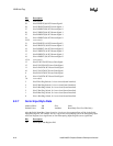
Intel® 460GX Chipset Software Developer’s Manual 8-13
WXB Hot-Plug
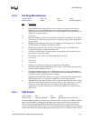
8.2.3 Hot-Plug Miscellaneous
Address Offset: 02h - 03h Size: 16 bits
Default Value: 0040h Attribute: Partial Read/Write
Bits
Description
15 reserved (0)
14 Enable SERR on Power Fault. When set, the assertion of a slot power fault causes a
SERR# to be asserted if SERR# generation is enabled in the PCI device command
register, the slot is connected to the bus or PCI clock, and IHPC power fault functions are
enabled (bit 10 of this register).
13 reserved (0)
12 Input Scan Complete. This bit is cleared at the conclusion of each input cycle. Software
can use this bit to determine when fresh data is available by setting it and waiting until a
logic 0 is seen.
11 66 MHz Prescaler Enable, Read Only, set according to the PCI frequency, a 1 indicates
the PCI frequency is 66 MHz, a 0 indicates 33 MHz.
10 Enable Power Fault Functions. This bit is also mapped to bit 13 of the IHPC Misc.
Configuration Register (configuration offset 42h).
9 Auto Power Down Disable. Controls whether or not opening a slot switch will cause a
powered slot to auto-power-down.
8 On / Off Busy status. (Same as Configuration Register 42, bit 0)
7 reserved (0)
6 reserved (1)
5 reserved (0)
4 Dummy Cycle Enable, this feature is not supported on this stepping.
3 General-interrupt-input Interrupt Pending. Set to a logic 1 when an interrupt is generated.
Cleared when the interrupt is cleared.
2 Shift Output Interrupt Pending / Clear. When read as logic 1, a hot-plug interrupt was
generated by SOBS changing from 1 to 0 while the Serial Output Interrupt Enable bit was
set. Writing a logic 1 clears this bit and its interrupt.
1 Shift Output Interrupt Enable. When set to a logic 1, an interrupt will be generated when
SOBS changes from 1 to 0, indicating completion of a serial output sequence.
0 Shift Output Go / Busy Status. Writing a logic 1 to this bit (after it has been read as a logic
0) initiates a serial output sequence (e.g. power-down of a slot). When read as a logic 0,
the previous serial output sequence has completed. Ensure that LED blinking has
completed (or is forced to complete) prior to initiating a SOGO for a slot power-up or
power-down.
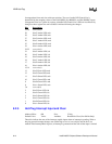
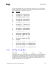
8.2.4 LED Control
Address Offset: 04h Size: 32 bits
Default Value: sampled at PWRGD Attribute: Read/Write (Pwr Good Rst Only)
If both the MSB and LSB for an LED are logic 0, then the LED is turned off. The LSB is for Blink
phase A and the MSB is for Blink phase B. Setting either phase A or phase B will program the
LED to blink. Setting both the MSB and the LSB will turn the LED on. An auto-power-down
sequence will turn off the LEDs for that slot. It is intended that the green LED is a power indicator
and the amber LED is the attention indicator.Following chip power on, all LED bits will be cleared


