


IFB Usage Considerations
10-18 Intel® 460GX Chipset Software Developer’s Manual
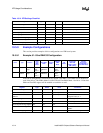
This register enables/disables bus master capability for the IDE function and provides direction
control for the IDE DMA transfers. This register also provides bits that software uses to indicate
DMA capability of the IDE device.
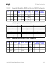
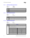
10.5.11.3 BMISX–Bus Master IDE Status Register (I/O)
Address Offset: Primary Channel–Base + 02h; Secondary Channel–Base + 0Ah
Default Value: 00h
Attribute: Read/Write Clear
This register provides status information about the IDE device and state of the IDE DMA transfer.
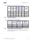
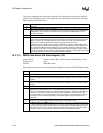
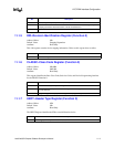
Bit Description
7:4 Reserved.
3 Bus Master Read/Write Control (RWCON). 0=Reads; 1=Writes. This bit must NOT be changed
when the bus master function is active. While a Ultra DMA transfer is in progress, this bit will be
READ ONLY. The bit will return to read/write once the synchronous DMA transfer has been
completed or halted.
2:1 Reserved.
0 Start/Stop Bus Master (SSBM). 1=Start; 0=Stop. When this bit is set to 1, bus master operation
starts. The controller transfers data between the IDE device and memory only while this bit is set.
Master operation can be stopped by writing a 0 to this bit. This results in all state information
being lost (i.e. master mode operation cannot be stopped and then resumed).
If this bit is set to 0 while bus master operation is still active (i.e. Bit 0=1 in the Bus Master IDE
Status Register for that IDE channel) and the drive has not yet finished its data transfer (bit 2=0 in
the channel’s Bus Master IDE Status Register), the bus master command is aborted and data
transferred from the drive may be discarded by IFB rather than being written to system memory.
This bit is intended to be set to 0 after the data transfer is completed, as indicated by either bit 0 or
bit 2 being set in the IDE Channel’s Bus Master IDE Status Register.
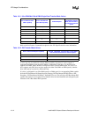
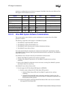
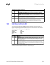
Bit Description
7 Reserved. This bit is hardwired to 0.
6 Drive 1 DMA Capable (DMA1CAP)–R/W. 1=Drive 1 is capable of DMA transfers. This bit is a
software controlled status bit that indicates IDE DMA device capability and does not affect hardware
operation.
5 Drive 0 DMA Capable (DMA0CAP)–R/W. 1=Drive 0 is capable of DMA transfers. This bit is a
software controlled status bit that indicates IDE DMA device capability and does not affect hardware
operation.
4:3 Reserved.
2 IDE Interrupt Status (IDEINTS)–R/WC. This bit, when set to a 1, indicates when an IDE device has
asserted its interrupt line. When bit 2=1, all read data from the IDE device has been transferred to
main memory and all write data has been transferred to the IDE device. Software sets this bit to a 0
by writing a 1 to it. IRQ14 is used for the primary channel and IRQ15 is used for the secondary
channel. Note that, if the interrupt status bit is set to a 0 by writing a 1 to this bit while the interrupt
line is still at the active level, this bit remains 0 until another assertion edge is detected on the
interrupt line.
1 IDE DMA Error–R/WC. This bit is set to 1 when IFB encounters a target abort or master abort while
transferring data on the PCI Bus. Software sets this bit to a 0 by writing a 1 to it.
0 Bus Master IDE Active (BMIDEA)–RO. IFB sets this bit to 1 when bit 0 in the BMICx Register is set
to 1. IFB sets this bit to 0 when the last transfer for a region is performed (where EOT for that region
is set in the region descriptor). IFB also sets this bit to 0 when bit 0 of the BMICx Register is set to 0.
When this bit is read as a zero, all data transferred from the drive during the previous bus master
command is visible in system memory, unless the bus master command was aborted.